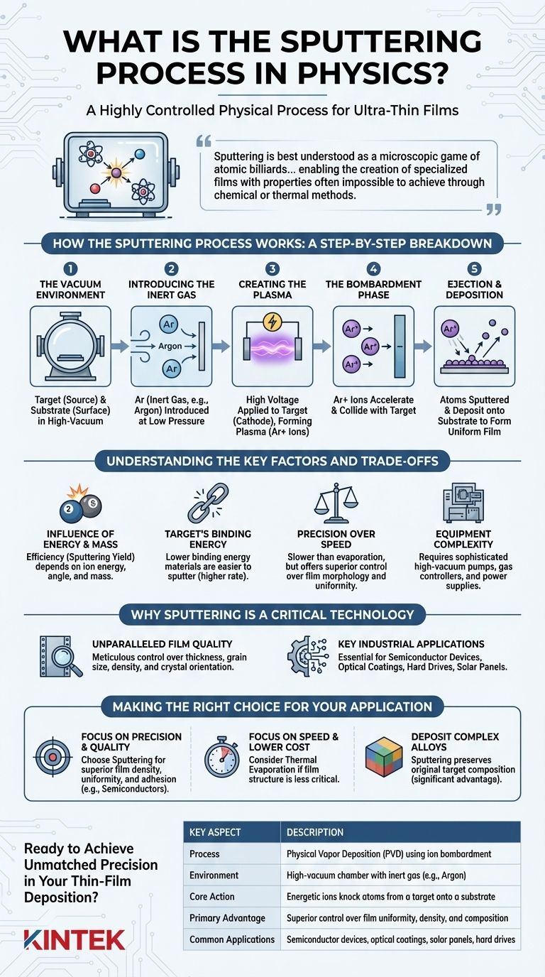
In essence, sputtering is a highly controlled physical process used to create ultra-thin films of material. It operates within a vacuum by bombarding a source material, called a target, with energetic ions. This collision has enough force to physically knock atoms loose from the target, which then travel and deposit onto a nearby surface, known as the substrate, forming a precise and uniform coating.
Sputtering is best understood as a microscopic game of atomic billiards. By using high-energy ions as "cue balls" to strike a target material, we gain precise control over the ejection and deposition of individual atoms, enabling the creation of specialized films with properties that are often impossible to achieve through chemical or thermal methods.
How the Sputtering Process Works: A Step-by-Step Breakdown
The sputtering process, while complex in its physics, follows a clear and logical sequence of events. Each step is critical for ensuring the quality and uniformity of the final thin film.
The Vacuum Environment
First, both the target (the source material) and the substrate (the surface to be coated) are placed inside a high-vacuum chamber. This vacuum is essential to remove air and other contaminants that could interfere with the process or become trapped in the film, compromising its purity.
Introducing the Inert Gas
An inert gas, most commonly Argon, is then introduced into the chamber at a very low pressure. This gas is not reactive and will not chemically bond with the target material; its sole purpose is to serve as the source for the bombarding particles.
Creating the Plasma
A high voltage is applied across the chamber, with the target material acting as the cathode (negative electrode). This voltage energizes free electrons, which collide with the neutral Argon atoms. These collisions knock electrons off the Argon atoms, creating positively charged Argon ions and forming a glowing, ionized gas known as a plasma.
The Bombardment Phase
Because they are positively charged, the Argon ions are now intensely attracted to the negatively charged target. They accelerate across the plasma and collide with the target's surface with significant kinetic energy. This is the core physical action of the process.
Ejection and Deposition
The momentum transfer from the ion collision is powerful enough to overcome the forces binding the target's atoms together. This causes microscopic particles—atoms or molecules—of the target material to be physically knocked out, or "sputtered," from the surface. These ejected particles travel through the vacuum and land on the substrate, gradually building up a thin, highly uniform film.
Understanding the Key Factors and Trade-offs
The effectiveness and outcome of sputtering are not random. They are governed by physical principles that can be controlled to achieve specific results. Understanding these factors is key to appreciating the technology's strengths and limitations.
The Influence of Energy and Mass
The efficiency of the process, known as the sputtering yield, depends heavily on the energy, angle, and mass of the bombarding ions. Higher energy ions generally eject more target atoms, but there is a point of diminishing returns.
The Target's Binding Energy
The nature of the target material itself is a critical factor. Materials with a lower binding energy—meaning their atoms are less tightly held together—are easier to sputter and will have a higher deposition rate.
Precision Over Speed
A significant trade-off with sputtering is its deposition rate. Compared to other methods like thermal evaporation, sputtering is generally a slower process. This is the price paid for superior control over the film's morphology, density, and uniformity.
Equipment Complexity
Sputtering systems require sophisticated and often expensive equipment, including high-vacuum pumps, precise gas flow controllers, and specialized power supplies. This complexity makes it an industrial-scale process rather than a simple benchtop technique.
Why Sputtering is a Critical Technology
The precise control offered by sputtering makes it an indispensable tool across science and high-tech industries. Its applications are widespread and are often found in devices we use every day.
Unparalleled Film Quality
Sputtering allows for meticulous control over film properties, including thickness, grain size, density, and even crystal orientation. This precision is essential for creating high-performance materials.
Key Industrial Applications
This technology is fundamental to modern manufacturing. It is used to produce semiconductor devices, create optical coatings on lenses (like anti-reflective layers), and deposit thin films for hard drives, solar panels, and other advanced nanotechnology products.
Making the Right Choice for Your Application
Selecting a deposition technique depends entirely on the requirements of the final product. Sputtering excels in applications where material properties are paramount.
- If your primary focus is precision and film quality: Sputtering offers superior control over film density, uniformity, and adhesion for demanding applications like semiconductors or optical coatings.
- If your primary focus is deposition speed and lower cost: Simpler methods like thermal evaporation may be more efficient for applications where film structure is less critical.
- If you need to deposit complex alloys or compounds: Sputtering is highly effective at preserving the original composition of the target material in the final film, a significant advantage over other methods.
Ultimately, understanding the physics of sputtering empowers you to leverage a process that transforms raw materials into high-performance technological surfaces, one atom at a time.
Summary Table:
| Key Aspect | Description |
|---|---|
| Process | Physical vapor deposition (PVD) using ion bombardment |
| Environment | High-vacuum chamber with inert gas (e.g., Argon) |
| Core Action | Energetic ions knock atoms from a target onto a substrate |
| Primary Advantage | Superior control over film uniformity, density, and composition |
| Common Applications | Semiconductor devices, optical coatings, solar panels, hard drives |
Ready to Achieve Unmatched Precision in Your Thin-Film Deposition?
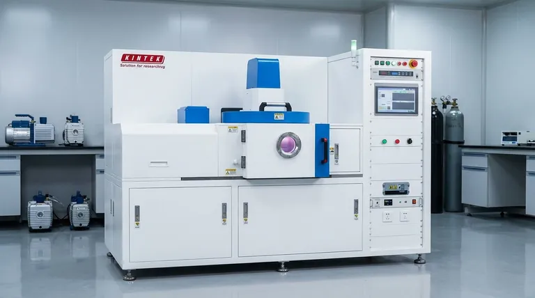
At KINTEK, we specialize in providing high-performance lab equipment, including advanced sputtering systems, to meet the exacting demands of modern laboratories and R&D facilities. Whether you are developing next-generation semiconductors, optical coatings, or nanotechnology products, our solutions deliver the superior film quality and control you need.
Let our experts help you select the right equipment to enhance your research and production capabilities. Contact KINTEK today to discuss your specific laboratory needs and discover how our sputtering technology can drive your innovations forward.
Visual Guide
Related Products
- Spark Plasma Sintering Furnace SPS Furnace
- Vacuum Induction Melting Spinning System Arc Melting Furnace
- Chemical Vapor Deposition CVD Equipment System Chamber Slide PECVD Tube Furnace with Liquid Gasifier PECVD Machine
- Customer Made Versatile CVD Tube Furnace Chemical Vapor Deposition Chamber System Equipment
People Also Ask
- What are the advantages of CAMI/SPS for W-Cu composite preparation? Reduce cycles from hours to seconds.
- Why are Spark Plasma Sintering (SPS) furnaces or hot presses utilized in the preparation of Li3PS4 solid electrolytes?
- What is the difference between spark plasma sintering and flash sintering? A Guide to Advanced Sintering Methods
- What is SPS sintering method? A Guide to High-Speed, High-Performance Material Fabrication
- What are the fundamentals of spark plasma sintering process? Unlock Rapid, High-Performance Material Consolidation


