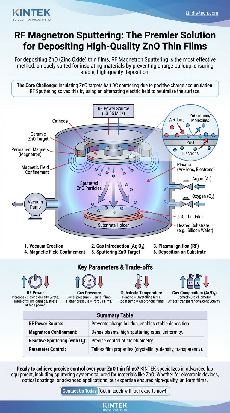
For depositing high-quality Zinc Oxide (ZnO) thin films, the most common and effective method is RF (Radio Frequency) Magnetron Sputtering. This technique is uniquely suited for materials like ZnO, which are electrical insulators or wide-bandgap semiconductors, because it prevents charge buildup on the target material, ensuring a stable and efficient deposition process with excellent film uniformity.
The core challenge in depositing an oxide material like ZnO is its insulating nature, which halts simpler DC sputtering processes. RF Magnetron Sputtering solves this by using an alternating electric field to neutralize the target surface, enabling consistent, high-rate deposition of dense and uniform films.
Why RF Magnetron Sputtering is the Standard for ZnO
The Challenge of Insulating Targets
Direct Current (DC) sputtering works well for conductive metal targets. However, when used with an insulating target like a ceramic ZnO wafer, a major problem arises.
The process bombards the target with positive ions (Argon, Ar+). On an insulator, these positive charges accumulate on the surface because they cannot be conducted away. This charge buildup eventually repels incoming Ar+ ions, extinguishing the plasma and stopping the sputtering process entirely.
The RF Solution: Alternating the Field
RF Sputtering uses a high-frequency power source, typically operating at 13.56 MHz. This rapidly alternates the electrical potential on the target.
During the negative cycle, the target attracts and is sputtered by positive ions, just like in DC sputtering. Crucially, during the brief positive cycle, the target attracts a flood of electrons from the plasma. These electrons neutralize the positive charge that built up during the negative cycle, effectively "resetting" the target surface and allowing the process to continue stably.
The Working Principle: A Step-by-Step Breakdown
To understand how the system works, imagine the process from start to finish. This explanation serves as a functional diagram of the components and their interactions.
Step 1: Creating a Vacuum
The entire process occurs inside a sealed vacuum chamber. The chamber is first pumped down to a very low pressure (high vacuum) to remove air and other contaminants like water vapor, which would otherwise interfere with the film's purity and properties.
Step 2: Introducing the Process Gas
A high-purity inert gas, almost always Argon (Ar), is introduced into the chamber. The pressure is carefully controlled and maintained at a low level, typically in the range of 1 to 100 mTorr.
Step 3: Igniting the Plasma
The RF power is applied to the electrode holding the ZnO target, known as the cathode. This high-frequency electric field energizes the Argon gas, stripping electrons from the Argon atoms and creating a plasma—a glowing cloud of positive Argon ions (Ar+) and free electrons.
Step 4: Magnetic Field Confinement (The "Magnetron")
This is the key to high efficiency. A set of powerful permanent magnets is placed behind the ZnO target. This magnetic field traps the highly mobile electrons in a path close to the target's surface.
By trapping the electrons, their path length is greatly increased, which dramatically increases the probability that they will collide with and ionize more neutral Argon atoms. This creates a much denser, more intense plasma precisely where it's needed, leading to a significantly higher sputtering rate.
Step 5: Sputtering the ZnO Target
The positively charged Ar+ ions in the dense plasma are accelerated by the electric field and smash into the surface of the ZnO target. This high-energy physical bombardment acts like a microscopic sandblaster, ejecting or "sputtering" atoms and molecules of ZnO from the target.
Step 6: Deposition onto the Substrate
The sputtered ZnO particles travel in straight lines from the target through the low-pressure environment until they strike the substrate (e.g., a silicon wafer or glass slide). Upon arrival, they condense and stick, gradually building up a thin film layer by layer.
Understanding the Key Parameters and Trade-offs
Achieving a specific ZnO film property—be it high conductivity, transparency, or crystallinity—requires precise control over several process variables.
Reactive Sputtering for Stoichiometry
Often, the sputtering process can cause the ZnO to lose some of its oxygen. To counteract this and ensure the final film is perfectly stoichiometric (an exact Zn:O ratio), a small, controlled amount of Oxygen (O2) is added to the Argon gas. This is known as reactive sputtering.
Critical Process Variables
- RF Power: Higher power increases the plasma density and the ion bombardment energy. This leads to a faster deposition rate but can also cause film damage or stress if too high.
- Gas Pressure: This affects the energy of the sputtered particles. Lower pressure results in fewer collisions and higher-energy deposition, often leading to denser films. Higher pressure can create more porous films.
- Substrate Temperature: Heating the substrate during deposition provides energy to the arriving atoms, allowing them to move around and settle into a more ordered, crystalline structure. Room temperature deposition often yields amorphous or poorly crystallized films.
- Gas Composition (Ar/O₂ Ratio): The amount of oxygen in the chamber is critical for controlling the film's stoichiometry, which in turn dictates its electrical and optical properties. Too little oxygen results in a metallic, non-transparent film; too much can slow the deposition rate.
Making the Right Choice for Your Goal
The ideal sputtering parameters are not universal; they depend entirely on the desired properties of the final ZnO film.
- If your primary focus is high crystallinity for electronic devices: You will need to use a higher substrate temperature (e.g., 200-400°C) and potentially a lower deposition rate to allow for optimal crystal growth.
- If your primary focus is high transparency for optical coatings: Your main concern will be precisely controlling the oxygen partial pressure to ensure full oxidation and minimize defects that absorb light.
- If your primary focus is high-speed industrial deposition: You will aim to maximize RF power and optimize gas pressure for the fastest possible rate while ensuring the film's uniformity remains within specification.
By mastering these principles, you gain precise control over the physical, electrical, and optical properties of your deposited ZnO thin films.
Summary Table:
| Feature | Benefit for ZnO Deposition |
|---|---|
| RF Power Source | Prevents charge buildup on insulating ZnO target, enabling stable deposition. |
| Magnetron Confinement | Creates a dense plasma for high sputtering rates and excellent film uniformity. |
| Reactive Sputtering (with O₂) | Allows precise control of stoichiometry for desired electrical/optical properties. |
| Parameter Control (Power, Pressure, Temp) | Tailors film properties like crystallinity, density, and transparency. |
Ready to achieve precise control over your ZnO thin films?
KINTEK specializes in advanced lab equipment, including sputtering systems tailored for materials like ZnO. Whether you're developing electronic devices, optical coatings, or other advanced applications, our expertise ensures you get the high-quality, uniform films you need.
Contact us today to discuss your specific requirements and let our solutions enhance your research and production outcomes. Get in touch with our experts now!
Visual Guide
Related Products
People Also Ask
- What is plasma chemical vapor deposition? A Low-Temperature Thin Film Coating Solution
- What is plasma enhanced chemical vapour deposition PECVD used for? Enable Low-Temp Thin Films for Electronics & Solar
- What is plasma enhanced chemical vapour deposition process? Unlock Low-Temperature, High-Quality Thin Films
- What is plasma CVD? Unlock Low-Temperature Thin Film Deposition for Sensitive Materials
- How does Radio Frequency Enhanced Plasma Chemical Vapour Deposition (RF-PECVD) work? Learn the Core Principles
