While specialized manufacturers like American Elements are known for producing sputtering targets, the more critical question is what separates a high-quality manufacturer from a standard supplier. The production of these components is a highly specialized field of materials science, where success is defined by extreme control over material purity, density, and microstructure.
The key is to understand that a sputtering target is not a simple piece of metal; it is a highly engineered component. Choosing a manufacturer is less about a brand name and more about their documented ability to control the precise material characteristics that directly impact the quality and consistency of your thin-film deposition process.
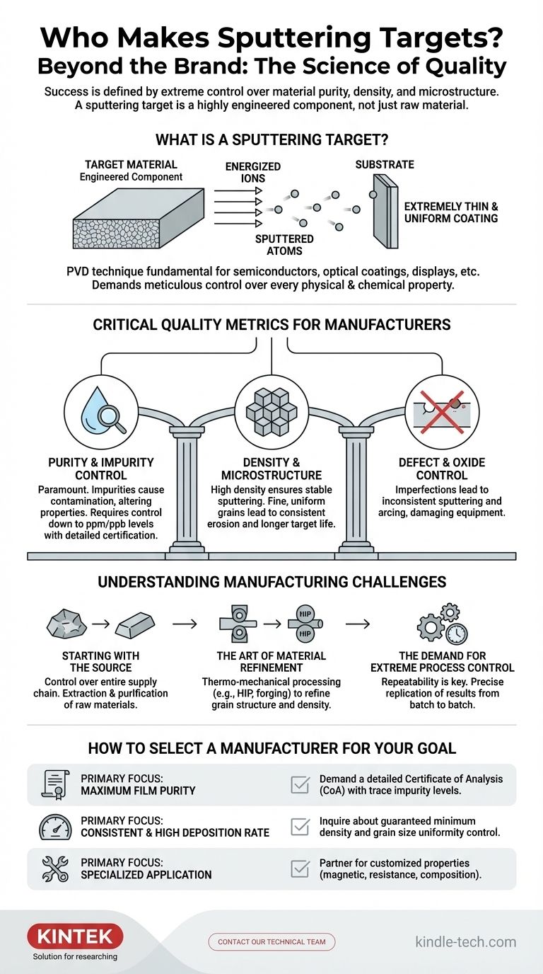
What is a Sputtering Target?
A Foundation of Modern Technology
Sputtering is a physical vapor deposition (PVD) technique, a process first discovered in the 19th century and developed for practical use in the 1920s. In this process, a target material is bombarded with energized ions, causing atoms to be "sputtered" or ejected from the target's surface.
These ejected atoms then travel and deposit onto a substrate, forming an extremely thin and uniform coating. This method is fundamental to manufacturing semiconductors, optical coatings, displays, and other advanced technological products.
Far More Than a Raw Material
A sputtering target has quality requirements that are orders of magnitude higher than those for traditional industrial materials. It is an engineered component where nearly every physical and chemical property is meticulously controlled.
This is because even minute inconsistencies in the target can translate into significant defects in the final thin film, compromising the performance and reliability of the end product.
Critical Quality Metrics for Manufacturers
Purity and Impurity Control
The purity of the target material is paramount. Any impurities within the target can be transferred to the deposited film, causing contamination that can alter its electrical, optical, or mechanical properties.
A reputable manufacturer must control impurity content down to the parts-per-million (ppm) or even parts-per-billion (ppb) level and provide detailed certification of their material's composition.
Density and Microstructure
High density is crucial for ensuring a stable and predictable sputtering rate. Low-density targets with voids or porosity can lead to inconsistent film deposition and the ejection of unwanted micro-droplets.
Similarly, the grain size and uniformity of the target's crystal structure directly influence how evenly the target erodes. A manufacturer's ability to create fine, uniform grains ensures a longer target lifespan and a more consistent deposition process.
Defect and Oxide Control
Internal defects or uncontrolled oxide content within the target material are significant failure points. These imperfections can lead to inconsistent sputtering rates and arcing—an unstable electrical discharge that can damage both the substrate and the equipment.
Understanding the Manufacturing Challenges
The Demand for Extreme Process Control
The primary challenge in manufacturing high-performance sputtering targets is repeatability. Achieving the required density and grain structure involves complex thermo-mechanical processing, and a manufacturer must be able to replicate these results precisely from one batch to the next.
Starting with the Source
The process begins with the extraction and purification of raw materials. A manufacturer cannot produce a 99.999% pure target if they begin with a contaminated or poorly refined source material. Control over the entire supply chain is a hallmark of a quality supplier.
The Art of Material Refinement
Through processes like hot isostatic pressing (HIP), forging, and rolling, manufacturers refine the material's grain structure. This thermo-mechanical treatment is what turns a simple metal ingot into a high-performance sputtering target with the desired density and uniformity.
How to Select a Manufacturer for Your Goal
When evaluating a sputtering target manufacturer, focus on their ability to deliver the specifications critical to your application.
- If your primary focus is maximum film purity: Demand a detailed Certificate of Analysis (CoA) that specifies the exact levels of trace impurities.
- If your primary focus is a consistent and high deposition rate: Inquire about their guaranteed minimum density and their process for controlling grain size uniformity.
- If your primary focus is a specialized application: Partner with a manufacturer who can customize properties like magnetic permeability, resistance, or composition for advanced materials like samarium cobalt alloys.
Ultimately, choosing the right manufacturer is about selecting a technical partner who understands and can control the material science behind your process.
Summary Table:
| Key Selection Criteria | Why It Matters for Your Application |
|---|---|
| Material Purity & Impurity Control | Ensures a contamination-free thin film, critical for electrical and optical properties. |
| High Density & Uniform Microstructure | Guarantees a stable sputtering rate, consistent deposition, and longer target life. |
| Defect & Oxide Control | Prevents arcing and process instability, protecting your substrate and equipment. |
| Repeatable Manufacturing Process | Delivers batch-to-batch consistency and reliability for your production line. |
Ready to achieve superior thin-film deposition?
Your application demands precision. KINTEK specializes in high-performance lab equipment and consumables, including sputtering targets engineered for maximum purity and consistency.
Let our expertise in material science become your advantage. Contact our technical team today to discuss your specific requirements.
Visual Guide
Related Products
- RF PECVD System Radio Frequency Plasma-Enhanced Chemical Vapor Deposition RF PECVD
- Aluminized Ceramic Evaporation Boat for Thin Film Deposition
- Vacuum Hot Press Furnace Machine for Lamination and Heating
- Vacuum Cold Trap Direct Cold Trap Chiller
- Cylindrical Resonator MPCVD Machine System Reactor for Microwave Plasma Chemical Vapor Deposition and Lab Diamond Growth
People Also Ask
- What are the advantages of PECVD? Enable Low-Temperature, High-Quality Thin-Film Deposition
- Why is PECVD environment friendly? Understanding the Eco-Friendly Benefits of Plasma-Enhanced Coating
- What are the benefits of PECVD? Achieve Superior Low-Temperature Thin Film Deposition
- How are PECVD and CVD different? A Guide to Choosing the Right Thin-Film Deposition Process
- What is plasma activated chemical vapour deposition method? A Low-Temperature Solution for Advanced Coatings