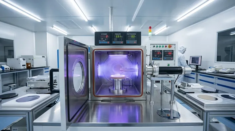
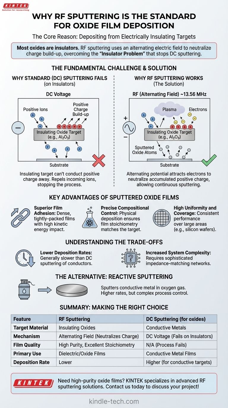
The fundamental reason RF sputtering is used for oxide films is its unique ability to deposit material from electrically insulating targets. Most oxide materials are poor electrical conductors, which prevents the use of simpler DC sputtering methods. RF sputtering overcomes this limitation by using an alternating electric field, making it the go-to technique for a vast range of dielectric and ceramic materials.
Sputtering is an exceptional process for creating high-quality thin films, but the target material's electrical properties dictate the specific technique required. RF sputtering's core advantage is that it neutralizes the charge build-up that would otherwise halt the process on insulating targets like oxides.
The Fundamental Challenge: Sputtering Insulators
To understand why RF sputtering is necessary, we must first look at why the standard, simpler method—DC sputtering—is incompatible with oxide materials.
How Standard (DC) Sputtering Works
In a direct current (DC) sputtering system, a high negative voltage is applied to the target material, which must be electrically conductive.
This negative potential attracts positively charged ions from the plasma. These ions accelerate and collide with the target, physically knocking off or "sputtering" atoms that then travel to and coat the substrate. This process requires a complete electrical circuit through the target.
The "Insulator Problem"
If you try to use an insulating target, like a ceramic oxide, in a DC system, the process fails almost immediately.
Positive ions from the plasma strike the target's surface, but because the material is an insulator, that positive charge cannot be conducted away. This rapid build-up of positive charge on the surface repels any further incoming positive ions, effectively stopping the sputtering process.
The RF Solution: An Alternating Field
RF (Radio Frequency) sputtering solves this problem by using an alternating power source, typically operating at 13.56 MHz.
Instead of a constant negative voltage, the target potential rapidly cycles between positive and negative. During the negative cycle, it attracts ions for sputtering, just as in the DC case. Critically, during the brief positive cycle, it attracts electrons from the plasma, which neutralize the positive charge that accumulated on the surface.
This continuous charge neutralization allows the sputtering of insulating materials to proceed without interruption.
Key Advantages of Sputtered Oxide Films
Beyond simply enabling the process, RF sputtering is chosen because it produces high-quality films with desirable properties essential for advanced applications.
Superior Film Adhesion
Sputtered particles possess high kinetic energy when they strike the substrate. This energy results in a dense, tightly-packed film that adheres very securely to the surface, a critical factor for durable optical and electronic devices.
Precise Compositional Control
Sputtering is a physical, not chemical, deposition process. This means the atomic composition of the sputtered film is extremely close to that of the target material. For complex oxides used in semiconductors and optics, this ensures the final film has the correct stoichiometry and desired properties.
High Uniformity and Coverage
The sputtering process provides excellent uniformity over large areas, such as silicon wafers or glass panels. This ensures consistent performance across the entire device, which is essential for manufacturing in the semiconductor and optical industries.
Understanding the Trade-offs
While powerful, RF sputtering is not without its considerations. Choosing a deposition technique always involves balancing performance with practicality.
Lower Deposition Rates
Generally, RF sputtering has a lower deposition rate compared to DC magnetron sputtering of conductive materials. This can impact manufacturing throughput and cost for high-volume production.
Increased System Complexity
RF power delivery systems require sophisticated impedance-matching networks to operate efficiently. This makes the equipment more complex and typically more expensive than its DC counterpart.
The Alternative: Reactive Sputtering
An alternative method to create oxide films is reactive DC sputtering. In this process, a conductive metal target is sputtered in a vacuum chamber that contains a mixture of argon and oxygen gas. The sputtered metal atoms react with the oxygen on their way to the substrate, forming an oxide film.
This can achieve higher deposition rates but often requires more complex process control to achieve the desired film stoichiometry.
Making the Right Choice for Your Goal
The decision to use RF sputtering hinges on your material requirements and production goals.
- If your primary focus is a high-purity, stoichiometric oxide film: RF sputtering from a ceramic oxide target is the most direct and reliable method.
- If your primary focus is the highest possible deposition rate for an oxide: Reactive DC sputtering from a metal target is a strong alternative, provided you can precisely control the reactive gas atmosphere.
- If your primary focus is depositing a conductive film (metal or conductive oxide): Standard DC magnetron sputtering is the faster, more efficient, and more cost-effective choice.
Ultimately, understanding the electrical nature of your target material is the key to selecting the most effective sputtering technique for your application.
Summary Table:
| Feature | RF Sputtering | DC Sputtering (for oxides) |
|---|---|---|
| Target Material | Insulating Oxides (e.g., Al2O3, SiO2) | Conductive Metals |
| Process Mechanism | Alternating RF field neutralizes surface charge | DC voltage requires conductive target |
| Film Quality | High purity, excellent stoichiometry, strong adhesion | N/A (Process fails) |
| Primary Use Case | High-quality dielectric/oxide films for optics, semiconductors | Conductive metal films |
| Deposition Rate | Lower | Higher (for conductive targets) |
Need to deposit high-purity oxide films with precise control? KINTEK specializes in advanced lab equipment, including RF sputtering systems, to help you achieve superior film quality for your semiconductor, optical, or research applications. Our experts can help you select the right sputtering technique for your specific oxide film requirements. Contact us today to discuss your project and discover how our solutions can enhance your laboratory's capabilities!
Visual Guide
Related Products
- RF PECVD System Radio Frequency Plasma-Enhanced Chemical Vapor Deposition RF PECVD
- Horizontal High Temperature Graphite Vacuum Graphitization Furnace
- Spark Plasma Sintering Furnace SPS Furnace
- Automatic Laboratory Hydraulic Press for XRF & KBR Pellet Press
- Electron Beam Evaporation Coating Oxygen-Free Copper Crucible and Evaporation Boat
People Also Ask
- How does plasma enhance CVD? Unlock Low-Temperature, High-Quality Film Deposition
- What is plasma enhanced chemical vapour deposition PECVD used for? Enable Low-Temp Thin Films for Electronics & Solar
- What is plasma CVD? Unlock Low-Temperature Thin Film Deposition for Sensitive Materials
- What is plasma enhanced chemical Vapour deposition process used for fabrication of? A Guide to Low-Temperature Thin Films
- What is plasma chemical vapor deposition? A Low-Temperature Thin Film Coating Solution


