Lab Materials
Erbium Fluoride (ErF3) Sputtering Target / Powder / Wire / Block / Granule
Item Number : LM-ErF3
Price varies based on specs and customizations
- Chemical Formula
- ErF3
- Purity
- 4N
- Shape
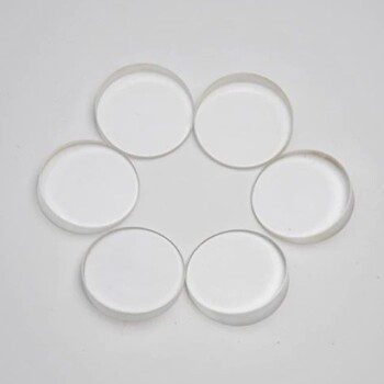
- discs / wire / block / powder / plates / column targets / step target / custom-made

Shipping:
Contact us to get shipping details Enjoy On-time Dispatch Guarantee.
We offer Erbium Fluoride (ErF3) materials at reasonable prices. Our expertise lies in producing and tailoring Erbium Fluoride (ErF3) materials of varying purities, shapes, and sizes to meet your unique requirements.
We offer a wide range of specifications and sizes for different types of materials, including sputtering targets (circular, square, tubular, irregular), coating materials, cylinders, cones, particles, foils, powders, 3D printing powders, nanometer powders, wire rods, ingots, and blocks, among others.
Details

About Erbium Fluoride (ErF3)
Erbium(III) fluoride (ErF3) is a rare earth metal fluoride compound that is used in the production of infrared light-transmitting and up-converting luminescent materials.
Moreover, Erbium Fluoride is an Erbium source that is insoluble in water, making it an ideal choice for oxygen-sensitive applications such as metal production. Fluoride compounds, in general, have numerous applications in modern technology, including oil refining, etching, synthetic organic chemistry, and pharmaceutical manufacturing.
For example, in 2013, researchers at the Max Planck Institute for Quantum Optics used Magnesium Fluoride to create a novel mid-infrared optical frequency comb composed of crystalline microresonators. This breakthrough has opened up possibilities for future advances in molecular spectroscopy.
Fluorides are also commonly used in metal alloying and optical deposition. Erbium Fluoride (ErF3) powder is readily available in most volumes, with ultra-high purity and high purity compositions enhancing both optical quality and scientific standards. Additionally, nanoscale elemental powders and suspensions can be used as alternative high surface area forms.
Ingredient Quality Control
- Raw material composition analysis
- Through the use of equipment such as ICP and GDMS, the content of metal impurities is detected and analyzed to ensure that it meets the purity standard;
Non-metallic impurities are detected by equipment such as carbon and sulfur analyzers, nitrogen and oxygen analyzers. - Metallographic flaw detection analysis
- The target material is inspected using flaw detection equipment to ensure that there are no defects or shrinkage holes inside the product;
Through metallographic testing, the internal grain structure of the target material is analyzed to ensure that the grains are fine and dense. - Appearance and dimension inspection
- Product dimensions are measured using micrometers and precision calipers to ensure compliance with drawings;
The surface finish and cleanliness of the product are measured using a surface cleanliness meter.
Conventional Sputtering Target Sizes
- Preparation process
- hot isostatic pressing, vacuum melting, etc.
- Sputtering target shape
- plane sputtering target, multi-arc sputtering target, step sputtering target, special-shaped sputtering target
- Round sputtering target size
- Diameter: 25.4mm / 50mm / 50.8mm / 60mm / 76.2mm / 80mm / 100mm / 101.6mm / 152.4mm
Thickness: 3mm / 4mm / 5mm / 6mm / 6.35mm
Size can be customized. - Square sputtering target size
- 50×50×3mm / 100×100×4mm / 300×300×5mm, size can be customized
Available Metal Forms
Metal Forms Details
We manufacture almost all the metals listed on the periodic table in a wide range of forms and purities, as well as standard sizes and dimensions. We can also produce custom-made products to meet specific customer requirements, such as size, shape, surface area, composition, and more. The following list provides a sample of the forms we offer, but it is not exhaustive. If you need laboratory consumables, please contact us directly to request a quote.
- Flat/Planar Forms: Board, Film, Foil, Microfoil, Microleaf, Paper, Plate, Ribbon, Sheet, Strip, Tape, Wafer
- Preformed Shapes: Anodes, Balls, Bands, Bars, Boats, Bolts, Briquettes, Cathodes, Circles, Coils, Crucibles, Crystals, Cubes, Cups, Cylinders, Discs, Electrodes, Fibers, Filaments, Flanges, Grids, Lenses, Mandrels, Nuts, Parts, Prisms, Pucks, Rings, Rods, Shapes, Shields, Sleeves, Springs, Squares, Sputtering Targets, Sticks, Tubes, Washers, Windows, Wires
- Microsizes: Beads, Bits, Capsules, Chips, Coins, Dust, Flakes, Grains, Granules, Micropowder, Needles, Particles, Pebbles, Pellets, Pins, Pills, Powder, Shavings, Shot, Slugs, Spheres, Tablets
- Macrosizes: Billets, Chunks, Cuttings, Fragments, Ingots, Lumps, Nuggets, Pieces, Punchings, Rocks, Scraps, Segments, Turnings
- Porous and Semi-Porous: Fabric, Foam, Gauze, Honeycomb, Mesh, Sponge, Wool
- Nanoscale: Nanoparticles, Nanopowders, Nanofoils, Nanotubes, Nanorods, Nanoprisms
- Others: Concentrate, Ink, Paste, Precipitate, Residue, Samples, Specimens
KinTek specializes in the manufacturing of high-purity and ultra-high-purity materials with a purity range of 99.999% (5N), 99.9999% (6N), 99.99995% (6N5), and in some cases, up to 99.99999% (7N). Our materials are available in specific grades, including UP/UHP, semiconductor, electronic, deposition, fiber optic, and MBE grades. Our high-purity metals, oxides, and compounds are specifically crafted to meet the rigorous demands of high-technology applications and are ideal for use as dopants and precursor materials for thin film deposition, crystal growth of semiconductors, and synthesis of nanomaterials. These materials find use in advanced microelectronics, solar cells, fuel cells, optical materials, and other cutting-edge applications.
Packaging
We use vacuum packaging for our high-purity materials, and each material has specific packaging tailored to its unique characteristics. For instance, our Hf sputter target is externally tagged and labeled to facilitate efficient identification and quality control. We take great care to prevent any damage that could occur during storage or transportation.
FAQ
What is Physical vapor deposition (PVD)?
What is sputtering target?
What are high purity materials?
What is magnetron sputtering?
How are sputtering targets made?
Why magnetron sputtering?
What is sputtering target used for?
What are the materials used in thin film deposition?
Thin film deposition commonly utilizes metals, oxides, and compounds as materials, each with its unique advantages and disadvantages. Metals are preferred for their durability and ease of deposition but are relatively expensive. Oxides are highly durable, can withstand high temperatures, and can be deposited at low temperatures, but can be brittle and challenging to work with. Compounds offer strength and durability, can be deposited at low temperatures and tailored to exhibit specific properties.
The selection of material for a thin film coating is dependent on the application requirements. Metals are ideal for thermal and electrical conduction, while oxides are effective in offering protection. Compounds can be tailored to suit specific needs. Ultimately, the best material for a particular project will depend on the specific needs of the application.
What are sputtering targets for electronics?
What are the methods to achieve optimal thin film deposition?
To achieve thin films with desirable properties, high-quality sputtering targets and evaporation materials are essential. The quality of these materials can be influenced by various factors, such as purity, grain size, and surface condition.
The purity of sputtering targets or evaporation materials plays a crucial role, as impurities can cause defects in the resulting thin film. Grain size also affects the quality of the thin film, with larger grains leading to poor film properties. Additionally, the surface condition is crucial, since rough surfaces can result in defects in the film.
To attain the highest quality sputtering targets and evaporation materials, it is crucial to select materials that possess high purity, small grain size, and smooth surfaces.
Uses of Thin Film Deposition
Zinc Oxide-Based Thin Films
ZnO thin films find applications in several industries such as thermal, optical, magnetic, and electrical, but their primary use is in coatings and semiconductor devices.
Thin-Film Resistors
Thin-film resistors are crucial for modern technology and are used in radio receivers, circuit boards, computers, radiofrequency devices, monitors, wireless routers, Bluetooth modules, and cell phone receivers.
Magnetic Thin Films
Magnetic thin films are used in electronics, data storage, radio-frequency identification, microwave devices, displays, circuit boards, and optoelectronics as key components.
Optical Thin Films
Optical coatings and optoelectronics are standard applications of optical thin films. Molecular beam epitaxy can produce optoelectronic thin-film devices (semiconductors), where epitaxial films are deposited one atom at a time onto the substrate.
Polymer Thin Films
Polymer thin films are used in memory chips, solar cells, and electronic devices. Chemical deposition techniques (CVD) offer precise control of polymer film coatings, including conformance and coating thickness.
Thin-Film Batteries
Thin-film batteries power electronic devices such as implantable medical devices, and the lithium-ion battery has advanced significantly thanks to the use of thin films.
Thin-Film Coatings
Thin-film coatings enhance the chemical and mechanical characteristics of target materials in various industries and technological fields. Anti-reflective coatings, anti-ultraviolet or anti-infrared coatings, anti-scratch coatings, and lens polarization are some common examples.
Thin-Film Solar Cells
Thin-film solar cells are essential to the solar energy industry, enabling the production of relatively cheap and clean electricity. Photovoltaic systems and thermal energy are the two main applicable technologies.
What is the lifetime of a sputtering target?
Factors and Parameters that Influence Deposition of Thin Films
Deposition Rate:
The rate at which the film is produced, typically measured in thickness divided by time, is crucial for selecting a technology suitable for the application. Moderate deposition rates are sufficient for thin films, while quick deposition rates are necessary for thick films. It is important to strike a balance between speed and precise film thickness control.
Uniformity:
The consistency of the film across the substrate is known as uniformity, which usually refers to film thickness but can also relate to other properties such as the index of refraction. It is important to have a good understanding of the application to avoid under- or over-specifying uniformity.
Fill Capability:
Fill capability or step coverage refers to how well the deposition process covers the substrate's topography. The deposition method used (e.g., CVD, PVD, IBD, or ALD) has a significant impact on step coverage and fill.
Film Characteristics:
The characteristics of the film depend on the application's requirements, which can be categorized as photonic, optical, electronic, mechanical, or chemical. Most films must meet requirements in more than one category.
Process Temperature:
Film characteristics are significantly affected by process temperature, which may be limited by the application.
Damage:
Each deposition technology has the potential to damage the material being deposited upon, with smaller features being more susceptible to process damage. Pollution, UV radiation, and ion bombardment are among the potential sources of damage. It is crucial to understand the limitations of the materials and tools.
4.7
out of
5
Quick delivery, excellent quality, and competitive pricing. Highly recommend!
4.8
out of
5
The product met all my expectations. I'm glad I chose KINTEK SOLUTION.
4.9
out of
5
Great product! It's of high quality and has been working perfectly for me.
4.9
out of
5
I'm impressed with the durability and performance of this product. Worth every penny!
4.6
out of
5
The product is exactly as advertised. I'm happy with my purchase.
4.8
out of
5
Excellent customer service and fast shipping. I'll definitely order again.
4.7
out of
5
The product is of exceptional quality and has exceeded my expectations.
4.9
out of
5
I highly recommend this product. It's a great value for the price.
4.8
out of
5
I'm very satisfied with the product's quality and performance.
4.7
out of
5
The product arrived on time and in perfect condition. I'm very pleased.
4.9
out of
5
This product is a game-changer. It has made my work so much easier.
4.6
out of
5
I'm glad I found this product. It's exactly what I needed.
REQUEST A QUOTE
Our professional team will reply to you within one business day. Please feel free to contact us!
Related Products

High Purity Erbium (Er) Sputtering Target / Powder / Wire / Block / Granule
Looking for high-quality Erbium materials for your lab? Look no further than our affordable selection of tailored Erbium products, available in a range of purities, shapes, and sizes. Shop sputtering targets, coating materials, powders, and more today!

High Purity Erbium Oxide (Er2O3) Sputtering Target / Powder / Wire / Block / Granule
Find high-quality Erbium Oxide (Er2O3) materials at competitive prices for your laboratory needs. Our tailored solutions in different purities, shapes, and sizes suit unique requirements. Browse our sputtering targets, coatings, powders, and more.

Ytterbium Fluoride (YbF3) Sputtering Target / Powder / Wire / Block / Granule
Buy high-quality Ytterbium Fluoride (YbF3) materials for your laboratory needs at affordable prices. We offer customized shapes and sizes, including sputtering targets, coating materials, powders, and more. Contact us today!

Cerium Fluoride (CeF3) Sputtering Target / Powder / Wire / Block / Granule
Looking for high-quality Cerium Fluoride materials? Our lab-grade CeF3 is available in a variety of shapes and sizes to meet your needs. Shop now for affordable prices!

Neodymium Fluoride (NdF3) Sputtering Target / Powder / Wire / Block / Granule
Looking for Neodymium Fluoride (NdF3) materials for your laboratory? We offer a wide range of options, from sputtering targets to powders, all customizable to meet your unique needs. Discover our affordable prices now.

Yttrium Fluoride (YF3) Sputtering Target / Powder / Wire / Block / Granule
Looking for high-quality Yttrium Fluoride (YF3) materials for laboratory use? Our affordable prices and expertise in producing custom shapes and sizes make us the ideal choice. Shop sputtering targets, coating materials, powders, and more today.

Dysprosium Fluoride (DyF3) Sputtering Target / Powder / Wire / Block / Granule
Looking for Dysprosium Fluoride (DyF3) materials for your lab? We produce and customize DyF3 materials of different purities, shapes, and sizes at reasonable prices. Find sputtering targets, coating materials, powders, and more. Contact us today.

Calcium Fluoride (CaF2) Sputtering Target / Powder / Wire / Block / Granule
Looking for high-quality Calcium Fluoride materials for laboratory use? Our expert team tailors different purities, shapes, and sizes to meet your specific needs. Browse our range of sputtering targets, coating materials, powders, and more. Get a quote today.

High Purity Europium (Eu) Sputtering Target / Powder / Wire / Block / Granule
Looking for high-quality Europium (Eu) materials for your lab? Check out our affordable options, tailored to your needs with various purities, shapes, and sizes. Choose from a range of sputtering targets, coating materials, powders, and more.

Lanthanum Fluoride (LaF3) Sputtering Target / Powder / Wire / Block / Granule
Looking for affordable Barium Titanate (LaF3) materials for your lab? Our tailored solutions fit your unique needs, with a wide range of shapes, sizes, and purities available. Explore our selection of sputtering targets, coating materials, powders, and more.
CaF2 substrate / window / lens
A CaF2 window is an optical window made of crystalline calcium fluoride. These windows are versatile, environmentally stable and resistant to laser damage, and they exhibit a high, stable transmission from 200 nm to about 7 μm.
Strontium Fluoride (SrF2) Sputtering Target / Powder / Wire / Block / Granule
Looking for Strontium Fluoride (SrF2) materials for your laboratory? Look no further! We offer a range of sizes and purities, including sputtering targets, coatings, and more. Order now at reasonable prices.

MgF2 magnesium fluoride crystal substrate / window
Magnesium fluoride (MgF2) is a tetragonal crystal that exhibits anisotropy, making it imperative to treat it as a single crystal when engaging in precision imaging and signal transmission.
Samarium Fluoride (SmF3) Sputtering Target / Powder / Wire / Block / Granule
Looking for high-quality Samarium Fluoride (SmF3) materials for your lab? Look no further! Our tailored solutions come in a range of purities, shapes, and sizes to suit your unique needs. Contact us today!

Sodium Fluoride (NaF) Sputtering Target / Powder / Wire / Block / Granule
Looking for Sodium Fluoride (NaF) materials? We offer tailored solutions of different purities, shapes, and sizes at affordable prices. Find sputtering targets, coating materials, powders, and more. Contact us today.

Magnesium Fluoride (MgF2) Sputtering Target / Powder / Wire / Block / Granule
Looking for high-quality Magnesium Fluoride (MgF2) materials for your laboratory needs? Look no further! Our expertly tailored materials come in a range of purities, shapes, and sizes to meet your specific requirements. Shop now for sputtering targets, powders, ingots, and more.
Potassium Fluoride (KF) Sputtering Target / Powder / Wire / Block / Granule
Get top-quality Potassium Fluoride (KF) materials for your lab needs at great prices. Our tailored purities, shapes, and sizes suit your unique requirements. Find sputtering targets, coating materials, and more.