Lab Materials
High Purity Erbium (Er) Sputtering Target / Powder / Wire / Block / Granule
Item Number : LM-ER
Price varies based on specs and customizations
- Chemical Formula
- Er
- Purity
- 3N
- Shape
- discs / wire / block / powder / plates / column targets / step target / custom-made

Shipping:
Contact us to get shipping details Enjoy On-time Dispatch Guarantee.
We offer Erbium (Er) materials for laboratory use at affordable prices. Our expertise lies in producing and customizing Erbium (Er) materials of varying purities, shapes, and sizes to meet your specific needs.
We provide a diverse selection of specifications and sizes for sputtering targets (circular, square, tubular, irregular), coating materials, cylinders, cones, particles, foils, powders, 3D printing powders, nanometer powders, wire rods, ingots, blocks, and more.
Details


About Erbium (Er)
Erbium is a versatile material with numerous applications in the field of materials science. This rare earth element is commonly used in glass coloring and can neutralize discoloring impurities, making it useful for eyewear and decorative glassware. Erbium is also a valuable component in fiber optics, where it serves as an amplifier for data transfer at the wavelength of 1.55 microns. Additionally, Erbium is used in lasers for medical and dental procedures.
Lasers based on Er:YAG have the ability to deliver energy without thermal build-up in tissue, making them ideal for surgical applications. Erbium is available in a variety of forms, including High Purity (99.999%) Erbium (Er) Sputtering Target, High Purity (99.999%) Erbium Oxide (Er2O3) Powder, and elemental or metallic forms such as pellets, rod, wire, and granules. Erbium oxides are commonly used for optical coating and thin film applications, while Erbium fluoride is useful in metallurgy, chemical and physical vapor deposition, and some optical coatings. Erbium is also available in soluble forms including chlorides, nitrates, and acetates, which can be manufactured as solutions at specified stoichiometries.
Ingredient Quality Control
- Raw material composition analysis
- Through the use of equipment such as ICP and GDMS, the content of metal impurities is detected and analyzed to ensure that it meets the purity standard;
Non-metallic impurities are detected by equipment such as carbon and sulfur analyzers, nitrogen and oxygen analyzers. - Metallographic flaw detection analysis
- The target material is inspected using flaw detection equipment to ensure that there are no defects or shrinkage holes inside the product;
Through metallographic testing, the internal grain structure of the target material is analyzed to ensure that the grains are fine and dense. - Appearance and dimension inspection
- Product dimensions are measured using micrometers and precision calipers to ensure compliance with drawings;
The surface finish and cleanliness of the product are measured using a surface cleanliness meter.
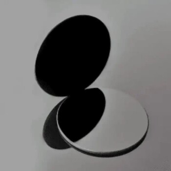
Conventional Sputtering Target Sizes
- Preparation process
- hot isostatic pressing, vacuum melting, etc.
- Sputtering target shape
- plane sputtering target, multi-arc sputtering target, step sputtering target, special-shaped sputtering target
- Round sputtering target size
- Diameter: 25.4mm / 50mm / 50.8mm / 60mm / 76.2mm / 80mm / 100mm / 101.6mm / 152.4mm
Thickness: 3mm / 4mm / 5mm / 6mm / 6.35mm
Size can be customized. - Square sputtering target size
- 50×50×3mm / 100×100×4mm / 300×300×5mm, size can be customized
Available Metal Forms
Metal Forms Details
We manufacture almost all the metals listed on the periodic table in a wide range of forms and purities, as well as standard sizes and dimensions. We can also produce custom-made products to meet specific customer requirements, such as size, shape, surface area, composition, and more. The following list provides a sample of the forms we offer, but it is not exhaustive. If you need laboratory consumables, please contact us directly to request a quote.
- Flat/Planar Forms: Board, Film, Foil, Microfoil, Microleaf, Paper, Plate, Ribbon, Sheet, Strip, Tape, Wafer
- Preformed Shapes: Anodes, Balls, Bands, Bars, Boats, Bolts, Briquettes, Cathodes, Circles, Coils, Crucibles, Crystals, Cubes, Cups, Cylinders, Discs, Electrodes, Fibers, Filaments, Flanges, Grids, Lenses, Mandrels, Nuts, Parts, Prisms, Pucks, Rings, Rods, Shapes, Shields, Sleeves, Springs, Squares, Sputtering Targets, Sticks, Tubes, Washers, Windows, Wires
- Microsizes: Beads, Bits, Capsules, Chips, Coins, Dust, Flakes, Grains, Granules, Micropowder, Needles, Particles, Pebbles, Pellets, Pins, Pills, Powder, Shavings, Shot, Slugs, Spheres, Tablets
- Macrosizes: Billets, Chunks, Cuttings, Fragments, Ingots, Lumps, Nuggets, Pieces, Punchings, Rocks, Scraps, Segments, Turnings
- Porous and Semi-Porous: Fabric, Foam, Gauze, Honeycomb, Mesh, Sponge, Wool
- Nanoscale: Nanoparticles, Nanopowders, Nanofoils, Nanotubes, Nanorods, Nanoprisms
- Others: Concentrate, Ink, Paste, Precipitate, Residue, Samples, Specimens
KinTek specializes in the manufacturing of high-purity and ultra-high-purity materials with a purity range of 99.999% (5N), 99.9999% (6N), 99.99995% (6N5), and in some cases, up to 99.99999% (7N). Our materials are available in specific grades, including UP/UHP, semiconductor, electronic, deposition, fiber optic, and MBE grades. Our high-purity metals, oxides, and compounds are specifically crafted to meet the rigorous demands of high-technology applications and are ideal for use as dopants and precursor materials for thin film deposition, crystal growth of semiconductors, and synthesis of nanomaterials. These materials find use in advanced microelectronics, solar cells, fuel cells, optical materials, and other cutting-edge applications.
Packaging
We use vacuum packaging for our high-purity materials, and each material has specific packaging tailored to its unique characteristics. For instance, our Hf sputter target is externally tagged and labeled to facilitate efficient identification and quality control. We take great care to prevent any damage that could occur during storage or transportation.
FAQ
What is Physical vapor deposition (PVD)?
What is sputtering target?
What are high purity materials?
What is magnetron sputtering?
What are high purity metals?
How are sputtering targets made?
Why magnetron sputtering?
What are high purity metals used for?
What is sputtering target used for?
What are the materials used in thin film deposition?
Thin film deposition commonly utilizes metals, oxides, and compounds as materials, each with its unique advantages and disadvantages. Metals are preferred for their durability and ease of deposition but are relatively expensive. Oxides are highly durable, can withstand high temperatures, and can be deposited at low temperatures, but can be brittle and challenging to work with. Compounds offer strength and durability, can be deposited at low temperatures and tailored to exhibit specific properties.
The selection of material for a thin film coating is dependent on the application requirements. Metals are ideal for thermal and electrical conduction, while oxides are effective in offering protection. Compounds can be tailored to suit specific needs. Ultimately, the best material for a particular project will depend on the specific needs of the application.
What are the benefits of using high-purity metals?
What are sputtering targets for electronics?
What are the methods to achieve optimal thin film deposition?
To achieve thin films with desirable properties, high-quality sputtering targets and evaporation materials are essential. The quality of these materials can be influenced by various factors, such as purity, grain size, and surface condition.
The purity of sputtering targets or evaporation materials plays a crucial role, as impurities can cause defects in the resulting thin film. Grain size also affects the quality of the thin film, with larger grains leading to poor film properties. Additionally, the surface condition is crucial, since rough surfaces can result in defects in the film.
To attain the highest quality sputtering targets and evaporation materials, it is crucial to select materials that possess high purity, small grain size, and smooth surfaces.
Uses of Thin Film Deposition
Zinc Oxide-Based Thin Films
ZnO thin films find applications in several industries such as thermal, optical, magnetic, and electrical, but their primary use is in coatings and semiconductor devices.
Thin-Film Resistors
Thin-film resistors are crucial for modern technology and are used in radio receivers, circuit boards, computers, radiofrequency devices, monitors, wireless routers, Bluetooth modules, and cell phone receivers.
Magnetic Thin Films
Magnetic thin films are used in electronics, data storage, radio-frequency identification, microwave devices, displays, circuit boards, and optoelectronics as key components.
Optical Thin Films
Optical coatings and optoelectronics are standard applications of optical thin films. Molecular beam epitaxy can produce optoelectronic thin-film devices (semiconductors), where epitaxial films are deposited one atom at a time onto the substrate.
Polymer Thin Films
Polymer thin films are used in memory chips, solar cells, and electronic devices. Chemical deposition techniques (CVD) offer precise control of polymer film coatings, including conformance and coating thickness.
Thin-Film Batteries
Thin-film batteries power electronic devices such as implantable medical devices, and the lithium-ion battery has advanced significantly thanks to the use of thin films.
Thin-Film Coatings
Thin-film coatings enhance the chemical and mechanical characteristics of target materials in various industries and technological fields. Anti-reflective coatings, anti-ultraviolet or anti-infrared coatings, anti-scratch coatings, and lens polarization are some common examples.
Thin-Film Solar Cells
Thin-film solar cells are essential to the solar energy industry, enabling the production of relatively cheap and clean electricity. Photovoltaic systems and thermal energy are the two main applicable technologies.
Which industries commonly use high-purity metals?
What is the lifetime of a sputtering target?
Factors and Parameters that Influence Deposition of Thin Films
Deposition Rate:
The rate at which the film is produced, typically measured in thickness divided by time, is crucial for selecting a technology suitable for the application. Moderate deposition rates are sufficient for thin films, while quick deposition rates are necessary for thick films. It is important to strike a balance between speed and precise film thickness control.
Uniformity:
The consistency of the film across the substrate is known as uniformity, which usually refers to film thickness but can also relate to other properties such as the index of refraction. It is important to have a good understanding of the application to avoid under- or over-specifying uniformity.
Fill Capability:
Fill capability or step coverage refers to how well the deposition process covers the substrate's topography. The deposition method used (e.g., CVD, PVD, IBD, or ALD) has a significant impact on step coverage and fill.
Film Characteristics:
The characteristics of the film depend on the application's requirements, which can be categorized as photonic, optical, electronic, mechanical, or chemical. Most films must meet requirements in more than one category.
Process Temperature:
Film characteristics are significantly affected by process temperature, which may be limited by the application.
Damage:
Each deposition technology has the potential to damage the material being deposited upon, with smaller features being more susceptible to process damage. Pollution, UV radiation, and ion bombardment are among the potential sources of damage. It is crucial to understand the limitations of the materials and tools.
4.9
out of
5
The Erbium sputtering target from KINTEK SOLUTION is a must-have for our laboratory. It's highly pure and produces consistent, high-quality thin films. We've seen a significant improvement in our research output since using it.
4.8
out of
5
As a lab manager, I'm always looking for ways to improve our efficiency and accuracy. KINTEK SOLUTION's Erbium sputtering target has been a game-changer for us. It's incredibly precise and has helped us reduce our production time significantly.
4.7
out of
5
The quality and purity of KINTEK SOLUTION's Erbium sputtering target are truly impressive. Our thin films have never looked better, and we've experienced a noticeable increase in their durability. Highly recommended!
4.8
out of
5
The Erbium sputtering target from KINTEK SOLUTION has exceeded our expectations. It's incredibly versatile and has allowed us to explore a wider range of applications in our research. A fantastic investment for any laboratory.
4.9
out of
5
KINTEK SOLUTION's Erbium sputtering target has revolutionized our thin film deposition process. Its exceptional purity and uniformity have resulted in remarkable improvements in the quality and performance of our devices. Highly satisfied!
4.7
out of
5
As a lab manager, I'm constantly seeking cost-effective solutions that don't compromise on quality. KINTEK SOLUTION's Erbium sputtering target fits the bill perfectly. It's not only affordable but also delivers exceptional results. Highly impressed!
4.8
out of
5
The Erbium sputtering target from KINTEK SOLUTION has been a valuable addition to our laboratory. Its high purity and consistent performance have enabled us to achieve remarkable precision and accuracy in our research. Highly recommended!
4.9
out of
5
KINTEK SOLUTION's Erbium sputtering target has been a lifesaver for our lab. Its exceptional quality and reliability have allowed us to streamline our research process and achieve groundbreaking results. A must-have for any laboratory striving for excellence.
4.7
out of
5
The Erbium sputtering target from KINTEK SOLUTION has been a game-changer for our thin film deposition experiments. Its superior purity and uniformity have resulted in remarkably improved film quality and enhanced device performance. Highly satisfied!
4.8
out of
5
KINTEK SOLUTION's Erbium sputtering target has been a revelation for our laboratory. Its exceptional purity and consistent performance have enabled us to achieve unprecedented levels of precision and accuracy in our research. Highly recommended!
REQUEST A QUOTE
Our professional team will reply to you within one business day. Please feel free to contact us!
Related Products

High Purity Erbium Oxide (Er2O3) Sputtering Target / Powder / Wire / Block / Granule
Find high-quality Erbium Oxide (Er2O3) materials at competitive prices for your laboratory needs. Our tailored solutions in different purities, shapes, and sizes suit unique requirements. Browse our sputtering targets, coatings, powders, and more.
Erbium Fluoride (ErF3) Sputtering Target / Powder / Wire / Block / Granule
Shop Erbium Fluoride (ErF3) materials of varying purities, shapes, and sizes for laboratory use. Our products include sputtering targets, coating materials, powders, and more. Browse now!
High Purity Cerium (Ce) Sputtering Target / Powder / Wire / Block / Granule
Looking for high-quality Cerium (Ce) materials for your laboratory? Our expertise lies in producing and tailoring materials of different purities, shapes, and sizes to suit your unique requirements. We offer a range of specifications and sizes, including sputtering targets, coating materials, powders, and more, all at reasonable prices.
High Purity Ytterbium (Yb) Sputtering Target / Powder / Wire / Block / Granule
Looking for Ytterbium (Yb) materials for your laboratory? Our expertise is in producing tailored Yb materials of various purities, shapes, and sizes. Choose from our wide range of specifications and sizes, including sputtering targets, coating materials, powders, and more. Affordable prices.

High Purity Europium (Eu) Sputtering Target / Powder / Wire / Block / Granule
Looking for high-quality Europium (Eu) materials for your lab? Check out our affordable options, tailored to your needs with various purities, shapes, and sizes. Choose from a range of sputtering targets, coating materials, powders, and more.

High Purity Terbium (Tb) Sputtering Target / Powder / Wire / Block / Granule
Buy high-quality Terbium (Tb) materials at affordable prices for your laboratory needs. We offer custom shapes, sizes, and purities to fit your unique requirements. Explore our range of sputtering targets, coatings, powders, and more.

High Purity Neodymium (Nd) Sputtering Target / Powder / Wire / Block / Granule
Looking for high-quality Neodymium (Nd) materials? Our lab-grade Nd materials come in a variety of purities, shapes, and sizes to suit your needs. Shop sputtering targets, coatings, particles, and more today.
High Purity Praseodymium (Pr) Sputtering Target / Powder / Wire / Block / Granule
Find high-quality Praseodymium (Pr) materials for laboratory use at reasonable prices. Our tailored products come in various sizes and purities, including sputtering targets, coating materials, and more. Contact us today.

High Purity Dysprosium (Dy) Sputtering Target / Powder / Wire / Block / Granule
Looking for high-quality Dysprosium (Dy) materials for your lab? Our tailored products come in different purities, shapes, and sizes to meet your unique needs. Explore our range of sputtering targets, powders, ingots, and more at reasonable prices.
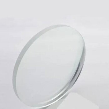
Infrared thermal imaging / infrared temperature measurement double-sided coated germanium (Ge) lens
Germanium lenses are durable, corrosion-resistant optical lenses suited for harsh environments and applications exposed to the elements.

High Purity Cerium Oxide (CeO2) Sputtering Target / Powder / Wire / Block / Granule
High-quality Cerium Oxide (CeO2) materials for laboratory use at affordable prices. Customizable shapes & sizes. Sputtering targets, powders, 3D printing powders & more. Order now!
High Purity Tungsten (W) Sputtering Target / Powder / Wire / Block / Granule
Find high-quality Tungsten (W) materials for your laboratory needs at affordable prices. We offer customized purities, shapes, and sizes of sputtering targets, coating materials, powders, and more.

Ytterbium Fluoride (YbF3) Sputtering Target / Powder / Wire / Block / Granule
Buy high-quality Ytterbium Fluoride (YbF3) materials for your laboratory needs at affordable prices. We offer customized shapes and sizes, including sputtering targets, coating materials, powders, and more. Contact us today!
High Purity Iridium (Ir) Sputtering Target / Powder / Wire / Block / Granule
Looking for high-quality Iridium (Ir) materials for laboratory use? Look no further! Our expertly produced and tailored materials come in various purities, shapes, and sizes to suit your unique needs. Check out our range of sputtering targets, coatings, powders, and more. Get a quote today!
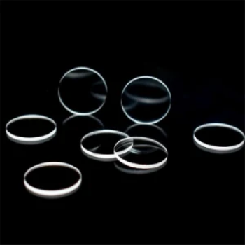
High temperature resistant optical quartz glass sheet
Discover the power of optical glass sheets for precise light manipulation in telecommunications, astronomy, and beyond. Unlock advancements in optical technology with exceptional clarity and tailored refractive properties.
High Purity Germanium (Ge) Sputtering Target / Powder / Wire / Block / Granule
Get high-quality gold materials for your laboratory needs at affordable prices. Our custom-made gold materials come in various shapes, sizes, and purities to fit your unique requirements. Explore our range of sputtering targets, coating materials, foils, powders, and more.
Optical ultra-clear glass sheet for laboratory K9 / B270 / BK7
Optical glass, while sharing many characteristics with other types of glass, is manufactured using specific chemicals that enhance properties crucial for optics applications.

Alkali-free / Boro-aluminosilicate glass
Boroaluminosilicate glass is highly resistant to thermal expansion, making it suitable for applications that require resistance to temperature changes, such as laboratory glassware and cooking utensils.

High Purity Yttrium Oxide (Y2O3) Sputtering Target / Powder / Wire / Block / Granule
Get high-quality Yttrium Oxide (Y2O3) materials tailored to your unique lab requirements. Our range includes sputtering targets, coating materials, powders, and more, all at reasonable prices.

High Purity Holmium (Ho) Sputtering Target / Powder / Wire / Block / Granule
Looking for affordable Holmium (Ho) materials for your laboratory? Our expertly produced and tailored range includes sputtering targets, powders, foils, and more - all available in a variety of sizes and shapes to fit your specific needs.