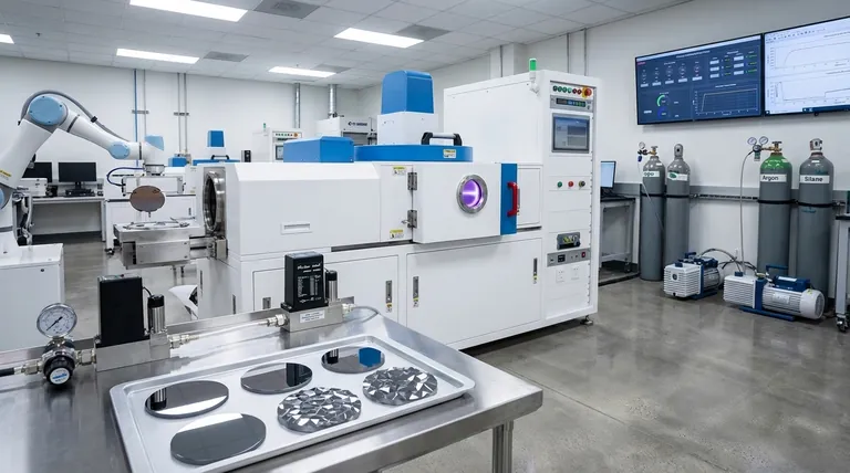
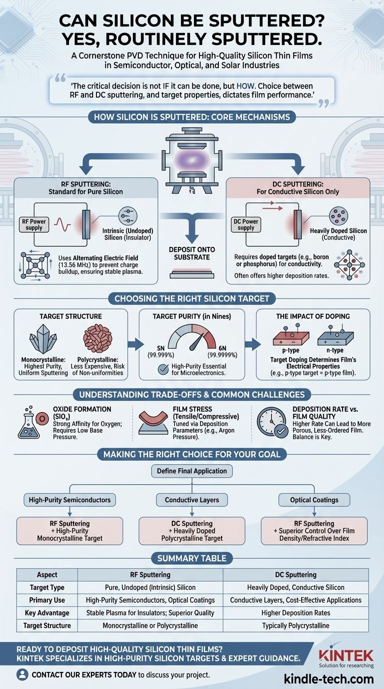
Yes, silicon is routinely sputtered. It is a cornerstone physical vapor deposition (PVD) technique used across the semiconductor, optical coating, and solar industries to create high-quality thin films of silicon. The process is highly controllable, allowing for precise engineering of the film's properties.
While sputtering silicon is a fundamental process, the critical decision is not if it can be done, but how. The choice between RF and DC sputtering, combined with the selection of a silicon target with the correct purity, crystal structure, and doping, directly dictates the final film's performance.
How Silicon is Sputtered: The Core Mechanisms
Sputtering is a vacuum deposition process where atoms are ejected from a solid target material after it is bombarded by energetic ions from a plasma. These ejected atoms then travel through the vacuum and deposit onto a substrate, forming a thin film.
RF Sputtering: The Standard for Pure Silicon
Because intrinsic (undoped) silicon is a semiconductor with high electrical resistivity, it behaves like an insulator in this context. It cannot sustain a direct current (DC) discharge.
Therefore, Radio Frequency (RF) sputtering is the standard method. The rapidly alternating electric field of the RF power supply (typically at 13.56 MHz) prevents positive charge from accumulating on the target surface, ensuring a stable plasma and a continuous sputtering process.
DC Sputtering: For Conductive Silicon Only
Direct Current (DC) sputtering can only be used if the silicon target is sufficiently conductive.
This is achieved by using heavily doped silicon targets, where impurities like boron (p-type) or phosphorus (n-type) have been added to dramatically lower the material's resistivity. DC sputtering often offers higher deposition rates than RF sputtering.
Choosing the Right Silicon Target
The "silicon" you sputter is not a generic material. The properties of the source target are critical for the resulting film.
Monocrystalline vs. Polycrystalline Targets
Monocrystalline (single crystal) silicon targets are cut from a large, perfect crystal ingot. They offer the highest purity and result in more uniform sputtering, which is critical for demanding semiconductor applications.
Polycrystalline silicon targets are made of many small, randomly oriented crystal grains. They are less expensive but can introduce minor non-uniformities and have a slightly higher risk of particle generation as grain boundaries sputter at different rates.
Understanding Target Purity
Silicon purity is measured in "nines." A "5N" target is 99.999% pure, while "6N" is 99.9999% pure. For most microelectronic and semiconductor applications, high-purity (5N or greater) silicon is essential to prevent unwanted contamination from affecting the film's electrical properties.
The Impact of Doping
The electrical characteristics of the sputtered silicon film are largely determined by the target's doping. Sputtering a boron-doped (p-type) target will produce a p-type film.
This allows engineers to deposit films with pre-determined resistivity and charge carrier types, which is essential for creating components like resistors, gates, or conductive layers within an integrated circuit.
Understanding the Trade-offs and Common Challenges
Sputtering silicon is a mature process, but success depends on managing key variables and potential pitfalls.
The Challenge of Oxide Formation
Silicon has a very strong affinity for oxygen. Any residual oxygen or water vapor in the vacuum chamber will readily react with the sputtered silicon atoms, both in transit and on the substrate surface.
This forms silicon oxide (SiOx) within the film, which can drastically alter its electrical and optical properties. Achieving a low base pressure in the vacuum system is critical for depositing pure silicon films.
Controlling Film Stress
Sputtered silicon films inherently develop internal stress, which can be either tensile (pulling apart) or compressive (pushing together). This stress arises from the deposition parameters, particularly the argon gas pressure.
High stress can cause the film to crack or delaminate from the substrate. Process engineers carefully tune sputtering pressure to find a "sweet spot" that minimizes stress while maintaining good film quality.
Deposition Rate vs. Film Quality
As a general rule, higher sputtering power leads to a higher deposition rate. However, this can come at the cost of film quality.
Aggressively high deposition rates can lead to a more porous film with a less-ordered atomic structure, potentially degrading its performance. The ideal parameters represent a balance between manufacturing throughput and the required film specifications.
Making the Right Choice for Your Goal
Your approach to sputtering silicon should be dictated entirely by the final application of the thin film.
- If your primary focus is high-purity semiconductor devices: Opt for RF sputtering with a high-purity (5N or better) monocrystalline silicon target to achieve the best film quality and electrical performance.
- If your primary focus is creating a conductive layer: DC sputtering with a heavily doped polycrystalline silicon target is a cost-effective and faster alternative for non-critical conductive films.
- If your primary focus is optical coatings: Use RF sputtering for its superior control over film density and refractive index, which are critical for optical performance.
Understanding these core principles transforms silicon sputtering from a simple deposition step into a precise engineering tool for creating functional materials.
Summary Table:
| Aspect | RF Sputtering | DC Sputtering |
|---|---|---|
| Target Type | Pure, undoped (intrinsic) silicon | Heavily doped, conductive silicon |
| Primary Use | High-purity semiconductor devices, optical coatings | Conductive layers, cost-effective applications |
| Key Advantage | Stable plasma for insulating targets; superior film quality | Higher deposition rates |
| Target Structure | Monocrystalline (high purity) or Polycrystalline | Typically Polycrystalline |
Ready to Deposit High-Quality Silicon Thin Films?
Whether you are developing advanced semiconductors, optical coatings, or solar cells, choosing the right sputtering method and target is critical for your film's performance. KINTEK specializes in providing high-purity silicon targets and expert guidance for your laboratory's specific needs.
Contact our experts today to discuss your project requirements and discover how our materials and support can help you achieve precise, reliable results.
Visual Guide
Related Products
- Silicon Carbide (SIC) Ceramic Sheet Wear-Resistant Engineering Advanced Fine Ceramics
- Laboratory CVD Boron Doped Diamond Materials
- Hemispherical Bottom Tungsten Molybdenum Evaporation Boat
- Silicon Carbide (SIC) Ceramic Sheet Flat Corrugated Heat Sink for Engineering Advanced Fine Ceramics
- Silicon Carbide (SIC) Ceramic Plate for Engineering Advanced Fine Ceramics
People Also Ask
- What are the properties of SiC? Unlock High-Temperature, High-Frequency Performance
- What are the uses of silicon carbide ceramics in different industries? Master Extreme Performance in Aerospace, Semiconductors & More
- What are the common uses of silicon carbide? Unlock Extreme Performance in Harsh Environments
- What is the strongest ceramics? Silicon Carbide Leads in Hardness & Thermal Strength
- What are the properties and applications of silicon carbide ceramics? Solve Extreme Engineering Challenges


