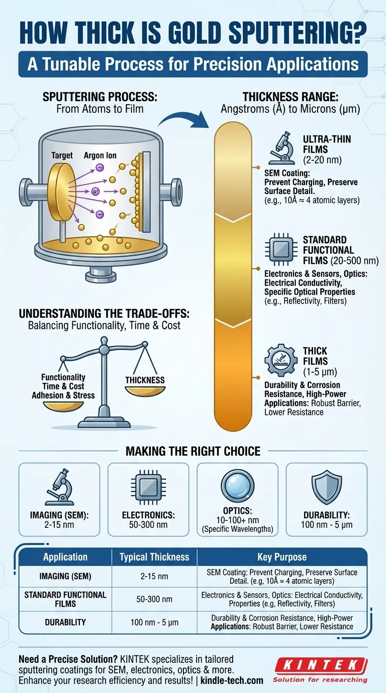
In practice, a gold layer applied by sputtering is exceptionally thin. The thickness is precisely controlled and typically ranges from a few angstroms (Å), which is equivalent to just a handful of atomic layers, up to a few microns (μm). This vast range allows the technique to be adapted for highly specific scientific and industrial applications.
The key takeaway is that gold sputtering is not about a single, standard thickness. It is a highly tunable deposition process where thickness is the primary variable, deliberately engineered to achieve a desired outcome—whether that's electrical conductivity, optical transparency, or surface preparation for imaging.

What is Gold Sputtering?
To understand the thickness, you must first understand the process. Gold sputtering is a Physical Vapor Deposition (PVD) method used to create a thin, uniform metallic film on a substrate.
The Core Mechanism
The process takes place in a vacuum chamber. High-energy ions, typically from an inert gas like argon, are accelerated and directed at a solid gold source known as a "target." This energetic bombardment ejects, or "sputters," individual gold atoms from the target.
From Atoms to Film
These liberated gold atoms travel through the vacuum and land on the substrate (the object being coated), gradually building up a film atom by atom. The result is an extremely uniform and dense coating that conforms precisely to the substrate's surface.
Demystifying the Thickness Range
The "angstroms to microns" range is vast. The specific thickness chosen is entirely dependent on the application.
The Angstrom to Nanometer Scale (Ultra-Thin Films)
An angstrom (Å) is one-tenth of a nanometer (nm). A 10 Å (1 nm) film is only about 4 atomic layers thick.
These ultra-thin films, typically 2 to 20 nm, are most famously used to coat non-conductive samples for Scanning Electron Microscopy (SEM). This thin layer is just enough to prevent electron charge buildup without obscuring the sample's surface details.
The Nanometer Scale (Standard Functional Films)
This is the most common range for functional applications. Thicknesses from 20 nm to 500 nm are standard in electronics, sensors, and optics.
In this range, the gold film provides excellent electrical conductivity for circuits and electrodes or specific optical properties like high reflectivity in the infrared spectrum.
The Micron Scale (Thick Films)
A micron (μm) is 1,000 nanometers. Reaching a thickness of 1 to 5 μm with sputtering is possible but less common, as it is a slow and expensive process.
These thicker films are reserved for applications demanding higher durability, lower electrical resistance for high-power applications, or a more robust corrosion-resistant barrier.
Understanding the Trade-offs
Choosing a sputtering thickness involves balancing competing technical and economic factors. The thickness you choose is always a compromise.
Thickness vs. Functionality
An ultra-thin 5 nm film is perfect for SEM because it's conductive yet semi-transparent to electrons, preserving surface detail. However, its electrical resistance would be too high for a sensor electrode.
Conversely, a 200 nm film offers excellent conductivity for an electrode but would completely obscure the fine details of a microscopic sample.
Thickness vs. Time and Cost
The relationship between time and thickness is nearly linear. Doubling the desired thickness will roughly double the process time and the consumption of the expensive gold target.
Achieving a micron-thick film can take hours, making it significantly more costly than depositing a nanometer-scale film, which might only take minutes.
Adhesion and Stress
As the film gets thicker, internal stresses can build up, potentially leading to poor adhesion or cracking. This is especially true for micron-scale films, which require careful process optimization to ensure they remain bonded to the substrate.
Making the Right Choice for Your Application
To select the correct thickness, you must first define your primary goal.
- If your primary focus is imaging (SEM): Aim for an ultra-thin layer of 2-15 nm. You need just enough conductivity to prevent charging without hiding surface features.
- If your primary focus is electronics (electrodes, contacts): A range of 50-300 nm is a common starting point, balancing excellent conductivity with reasonable cost and processing time.
- If your primary focus is optics (mirrors, filters): Thickness is critical and highly specific to the desired wavelength; it could be anything from 10 nm to over 100 nm depending on the required reflectivity or transmission.
- If your primary focus is durability or corrosion resistance: You will likely need a thicker film, starting from several hundred nanometers and potentially extending into the low micron range.
Ultimately, the thickness of a sputtered gold layer is not a fixed value but a precisely engineered parameter designed to meet the demands of your specific scientific or industrial goal.
Summary Table:
| Application | Typical Thickness Range | Key Purpose |
|---|---|---|
| SEM Coating | 2 - 20 nm | Prevent charging, preserve detail |
| Electronics & Sensors | 20 - 500 nm | Electrical conductivity, electrodes |
| Optics (Mirrors/Filters) | 10 - 100+ nm | Specific reflectivity/transmission |
| Durability/Corrosion Resistance | 100 nm - 5 μm | Robust barrier, lower resistance |
Need a precise gold sputtering solution for your lab? KINTEK specializes in lab equipment and consumables, delivering tailored sputtering coatings for SEM, electronics, optics, and more. Our expertise ensures optimal thickness, adhesion, and performance for your specific application—enhancing your research efficiency and results. Contact us today to discuss your project requirements!
Visual Guide
Related Products
- Electron Beam Evaporation Coating Gold Plating Tungsten Molybdenum Crucible for Evaporation
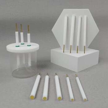
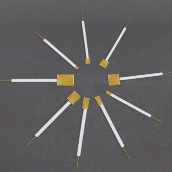
- Gold Disc Electrode
- Gold Electrochemical Sheet Electrode Gold Electrode
- Spark Plasma Sintering Furnace SPS Furnace
People Also Ask
- What are the applications of e-beam evaporation? Achieve High-Purity Coatings for Optics & Electronics
- What is the current of e-beam evaporation? A Guide to High-Purity Thin Film Deposition
- What is e-beam evaporation? Achieve High-Purity Thin Film Deposition for Your Lab
- What materials are used in electron beam evaporation? Master High-Purity Thin Film Deposition
- How is an electron beam evaporator cooled during deposition? Essential Thermal Management for Stable Processes