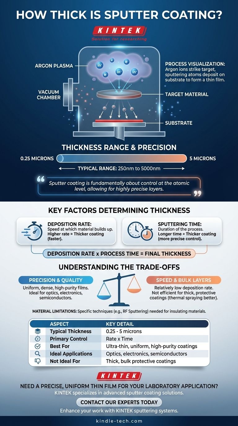
In short, sputter coating is a thin-film deposition technique. The resulting coating thickness typically ranges from 0.25 microns to 5 microns. This process is designed for precision and uniformity over very small scales, not for creating thick, bulk layers of material.
Sputter coating is fundamentally about control at the atomic level. The final thickness is not a fixed property but a direct result of process duration and deposition rate, allowing for highly precise layers measured in nanometers or microns.
How Sputter Coating Works
The Core Mechanism
Sputter coating is a physical vapor deposition (PVD) process that takes place in a vacuum. It begins by introducing an inert gas, typically argon, into a vacuum chamber.
A high voltage is applied, causing the argon gas to form a plasma of positively charged ions.
From Target to Substrate
These energetic argon ions are accelerated toward a source material, known as the target. When the ions strike the target, they physically knock off, or "sputter," atoms of the target material.
These sputtered atoms travel through the vacuum and deposit onto the desired object, called the substrate, forming a thin, uniform film.
Key Factors Determining Thickness
Deposition Rate
The primary factor controlling thickness is the deposition rate. This is the speed at which material is sputtered from the target and builds up on the substrate.
Older methods like simple DC sputtering suffered from low deposition rates, making the process very slow. Modern systems have improved this, but it remains a key variable.
Sputtering Time
The final thickness is a direct function of the deposition rate multiplied by the process time. To create a thicker coating, you simply run the process for a longer duration.
This linear relationship allows for extremely precise control over the final film thickness, which is critical for applications in optics and electronics.
Understanding the Trade-offs
Precision Over Speed
The key advantage of sputter coating is its ability to create exceptionally uniform, dense, and high-purity films with precise thickness control.
However, this precision comes at the cost of speed. Compared to other coating methods like thermal spraying, sputter coating has a relatively low deposition rate. It is not an efficient method for applying thick, protective layers.
Material Limitations
While modern techniques have expanded the range of sputterable materials, the process was historically limited. Simple DC sputtering, for instance, cannot be used on insulating materials.
This limitation has been largely overcome with technologies like RF (Radio Frequency) sputtering, but it highlights that the specific technique must be matched to the material being deposited.
Making the Right Choice for Your Goal
The suitability of sputter coating depends entirely on your application's requirements for thickness and precision.
- If your primary focus is an ultra-thin, highly uniform layer for optics or electronics: Sputter coating is an ideal choice due to its exceptional control and quality.
- If your primary focus is a thick, durable coating for wear or corrosion resistance: Other methods like thermal spraying or electroplating may be more practical and cost-effective.
- If your primary focus is coating an insulating material like a ceramic: You must ensure the specific sputtering technique, such as RF sputtering, is capable of handling non-conductive targets.
Ultimately, understanding that sputter coating excels at precision allows you to select it for the applications where it truly shines.
Summary Table:
| Aspect | Key Detail |
|---|---|
| Typical Thickness Range | 0.25 to 5 microns (250 to 5000 nanometers) |
| Primary Control Factor | Deposition Rate x Process Time |
| Best For | Ultra-thin, uniform, high-purity coatings |
| Ideal Applications | Optics, electronics, semiconductors |
| Not Ideal For | Thick, bulk protective coatings |
Need a precise, uniform thin film for your laboratory application? KINTEK specializes in lab equipment and consumables, providing advanced sputter coating solutions that deliver the controlled thickness and high-quality results your research demands. Contact our experts today to discuss how our sputtering systems can enhance your work!
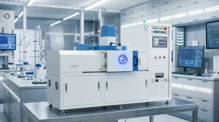
Visual Guide
Related Products
- Infrared Transmission Coating Sapphire Sheet Substrate Window
- Electron Beam Evaporation Coating Oxygen-Free Copper Crucible and Evaporation Boat
- 400-700nm Wavelength Anti Reflective AR Coating Glass
- Custom CVD Diamond Coating for Lab Applications
- Molybdenum Tungsten Tantalum Special Shape Evaporation Boat
People Also Ask
- What is organic thin film? A Guide to Engineered Molecular Layers for Advanced Tech
- What is the optical coating? Master Light Control for Superior Optical Performance
- Why do we need optical coating? To Control Light and Enhance Optical Performance
- What are the applications of optical coating? Unlock Advanced Light Control for Your Industry
- How do cooling jackets or heat exchangers contribute to the stability of glycerol conversion? Master Thermal Management


