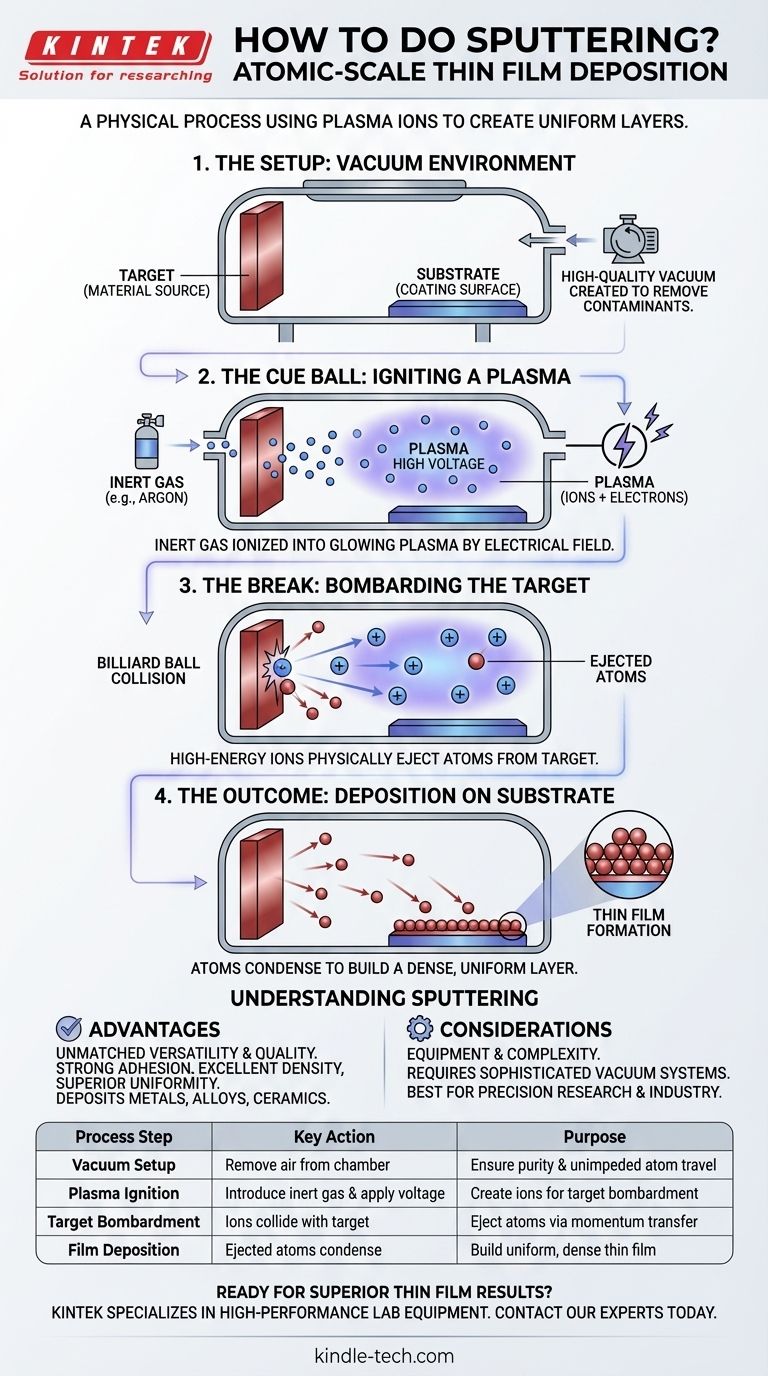
At its core, sputtering is a physical process used to deposit an ultra-thin layer of material onto a surface. The method involves creating a vacuum, introducing an inert gas to form a plasma, and using ions from that plasma to bombard a source material, or "target." This collision ejects atoms from the target, which then travel and coat a nearby substrate, forming a highly uniform and adhesive thin film.
Sputtering is not a simple chemical reaction but a controlled, atomic-scale collision. The entire process hinges on using high-energy ions to physically knock atoms off a target material, which then deposit onto a substrate in a highly predictable and controlled vacuum environment.
The Core Principle: A Billiard Ball Collision at the Atomic Scale
Sputtering is a form of physical vapor deposition (PVD). The most effective way to understand it is to imagine a game of billiards, but at an atomic level.
The Setup: Creating a Controlled Environment
Before any sputtering occurs, the system must be prepared. This involves placing the target (the material you want to deposit) and the substrate (the surface you want to coat) inside a vacuum chamber.
A high-quality vacuum is created to remove air and other contaminants. This ensures the purity of the final film and allows the sputtered atoms to travel unimpeded from the target to the substrate.
The Cue Ball: Igniting a Plasma
Once a vacuum is established, a small, controlled amount of an inert gas—most commonly Argon—is introduced into the chamber.
A strong electrical field (voltage) is then applied. This high energy strips electrons from the Argon atoms, creating a glowing, ionized gas known as a plasma. This plasma consists of positively charged Argon ions and free electrons.
The Break: Bombarding the Target
The negatively charged target material attracts the positively charged Argon ions from the plasma, causing them to accelerate and collide with the target's surface at high speed.
This high-energy bombardment transfers momentum and energy, physically knocking atoms or molecules out of the target material. This ejection of target atoms is the "sputtering" phenomenon itself.
The Outcome: Deposition on the Substrate
The ejected target atoms travel in a straight line from the target. They eventually strike the strategically placed substrate.
Upon arrival, these atoms condense on the substrate's surface, gradually building up layer by layer to form a thin, dense, and uniform film. The process is precisely controlled by factors like time and power to achieve a specific film thickness.
Understanding the Advantages and Trade-offs
Sputtering is a powerful technique, but it's essential to understand its strengths and the context in which it operates.
The Advantage: Unmatched Versatility and Quality
The primary benefit of sputtering is the exceptional quality and control it offers. It produces thin films with strong adhesion, excellent density, and superior uniformity across the substrate.
Furthermore, because it is a physical and not a chemical process, it is incredibly versatile. It can be used to deposit a vast range of materials, including metals, alloys, ceramics, and other insulating materials, onto virtually any type of substrate.
The Consideration: Equipment and Complexity
Sputtering is not a simple benchtop procedure. It requires sophisticated vacuum equipment and often necessitates a cleanroom facility to prevent contamination and ensure high-quality results.
This complexity means it is a process best suited for industrial and research applications where precision, purity, and repeatability are critical, such as in semiconductor manufacturing or the creation of precision optics.
Making the Right Choice for Your Goal
Sputtering is chosen when the material properties of the final thin film are paramount.
- If your primary focus is high-quality, dense coatings: Sputtering is an ideal choice due to its ability to produce films with excellent adhesion and uniformity.
- If your primary focus is depositing complex or non-conductive materials: The physical nature of sputtering makes it a superior choice for depositing alloys, ceramics, and insulators that are difficult to handle with other methods.
- If your primary focus is repeatable, industrial-scale production: Sputtering's high degree of process control makes it a reliable and reproducible method for mass manufacturing applications.
Ultimately, sputtering provides a precise and powerful method for engineering the surfaces of materials at the atomic level.
Summary Table:
| Process Step | Key Action | Purpose |
|---|---|---|
| Vacuum Setup | Remove air from the chamber | Ensure purity and unimpeded atom travel |
| Plasma Ignition | Introduce inert gas (e.g., Argon) and apply voltage | Create ions for target bombardment |
| Target Bombardment | Ions collide with the target material | Eject atoms via physical momentum transfer |
| Film Deposition | Ejected atoms travel and condense on the substrate | Build a uniform, dense thin film layer by layer |
Ready to achieve superior thin film results with precision sputtering equipment?
KINTEK specializes in high-performance lab equipment and consumables for all your sputtering and thin film deposition needs. Whether you are in research or industrial-scale production, our solutions deliver the repeatability, purity, and control required for exceptional coatings.
Contact our experts today to discuss how we can support your laboratory's specific requirements and help you engineer materials at the atomic level.
Visual Guide
Related Products
- Spark Plasma Sintering Furnace SPS Furnace
- Vacuum Induction Melting Spinning System Arc Melting Furnace
- Chemical Vapor Deposition CVD Equipment System Chamber Slide PECVD Tube Furnace with Liquid Gasifier PECVD Machine
- Customer Made Versatile CVD Tube Furnace Chemical Vapor Deposition Chamber System Equipment
People Also Ask
- What is the process fundamentals of spark plasma sintering? Achieve Rapid, High-Density Material Consolidation
- What is the difference between spark plasma sintering and flash sintering? A Guide to Advanced Sintering Methods
- What is the theory of spark plasma sintering? A Guide to Rapid, Low-Temperature Densification
- What is SPS sintering method? A Guide to High-Speed, High-Performance Material Fabrication
- What are the advantages of CAMI/SPS for W-Cu composite preparation? Reduce cycles from hours to seconds.


