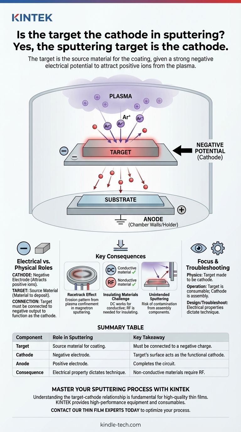
For all practical purposes, yes, the sputtering target is the cathode. The target is the source material for the coating, and it is given a strong negative electrical potential (making it the cathode) to attract positive ions from the plasma. These high-energy ions strike the target, ejecting atoms that then deposit onto your substrate.
The critical concept is one of function, not just name. For sputtering to work, the target material must serve as the negative electrode (the cathode) to attract the energized ions that do the sputtering. While the "cathode" can sometimes refer to the larger assembly that holds the target, the target's surface is where the essential action occurs.
The Roles of Cathode, Anode, and Target
To truly grasp the process, it's essential to separate the electrical roles from the physical components. The confusion often arises when these terms are used interchangeably.
The Cathode: The Negative Electrode
In any DC electrical circuit, the cathode is the electrode with a negative potential. Its role is to attract positively charged ions (cations) or to emit electrons. In sputtering, its primary role is to attract the positive ions.
The Target: The Source Material
The target is simply a physical block or plate of the material you wish to deposit as a thin film. This could be titanium, gold, silicon dioxide, or any number of other materials.
Connecting the Electrical to the Physical
For sputtering to happen, you must bombard the target material with high-energy ions. Since these ions (typically from an inert gas like Argon) are positively charged (Ar+), they must be accelerated toward a negative charge.
Therefore, the target is intentionally connected to the negative output of a power supply, forcing it to function as the cathode of the plasma circuit. The chamber walls or a dedicated substrate holder are typically grounded, acting as the anode (the positive electrode).
Why Terminology Can Be Confusing
The apparent contradiction in terms often comes from the difference between simple and complex sputtering systems.
In Simple DC Sputtering
In the most basic diode sputtering setup, the target plate itself is often the entire cathode. The terms are one and the same. It's a single, negatively charged component that is the source of the sputtered material.
In Magnetron Sputtering
Modern systems, particularly magnetron sputtering systems, use more complex assemblies. Here, the "cathode" often refers to the entire water-cooled, magnetic assembly that is installed in the chamber.
The "target" is then the consumable plate of material that you bolt onto the face of this cathode assembly. In this context, an engineer might say the cathode is "behind" the target, but electrically, the target's surface is still the functioning face of the cathode.
Key Consequences of This Setup
Understanding that the target is the cathode has direct, practical implications for the sputtering process.
The "Racetrack" Effect
In magnetron sputtering, magnets behind the target confine the plasma to a specific area to increase sputtering efficiency. This causes the target to erode unevenly in a distinct pattern, often called a "racetrack," where the plasma is most dense.
The Challenge of Insulating Materials
Because the target must hold a negative charge, standard DC sputtering only works for conductive materials (like metals). If you use a non-conductive (dielectric) target, positive charge from the arriving ions builds up on its surface, neutralizing the negative potential and stopping the sputtering process. This is why a different technique, RF Sputtering, is required for insulating materials.
Unintended Sputtering and Contamination
Any surface held at a cathode potential can be sputtered. If the target is not properly sized or shielded, the plasma can begin to sputter the metallic components of the cathode assembly or clamps holding the target. This can introduce impurities into your thin film.
Making the Right Choice for Your Goal
Your understanding of this concept should adapt to your specific task.
- If your primary focus is understanding the physics: Think of the target as the component that is made to be the cathode. Its negative potential is the engine that drives the entire process.
- If your primary focus is operating the equipment: Be precise with your terms. "Target" refers to the consumable material you change, while "cathode" (or "gun") may refer to the permanent assembly it mounts to.
- If your primary focus is process design or troubleshooting: Remember that the target's electrical properties are paramount. A material's conductivity dictates whether you can use DC or must use RF sputtering.
Ultimately, knowing that the target's surface functions as the electrical cathode is the key to mastering and troubleshooting the sputtering process.
Summary Table:
| Component | Role in Sputtering | Key Takeaway |
|---|---|---|
| Target | Source material for the thin film coating. | Must be connected to a negative charge to function. |
| Cathode | The negative electrode that attracts positive ions. | The target's surface acts as the functional cathode. |
| Anode | The positive electrode (usually chamber walls). | Completes the electrical circuit. |
| Consequence | For DC sputtering, the target material must be conductive. | Non-conductive (insulating) materials require RF sputtering. |
Master Your Sputtering Process with KINTEK
Understanding the intricate relationship between your target material and the cathode is fundamental to achieving high-quality, contamination-free thin films. Whether you are working with conductive metals or insulating ceramics, selecting the right equipment and configuration is critical.
KINTEK specializes in high-performance lab equipment and consumables, including sputtering targets and cathode assemblies, tailored to meet the precise needs of your laboratory. Our experts can help you optimize your process, avoid contamination, and select the correct sputtering technique for your specific materials.
Contact our thin film experts today to discuss your sputtering requirements and discover how KINTEK's solutions can enhance your research and production outcomes.
Visual Guide
Related Products
- Reference Electrode Calomel Silver Chloride Mercury Sulfate for Laboratory Use
- Multifunctional Electrolytic Electrochemical Cell Water Bath Single Layer Double Layer
- Molybdenum Tungsten Tantalum Special Shape Evaporation Boat
- Hemispherical Bottom Tungsten Molybdenum Evaporation Boat
- Cylindrical Press Mold with Scale for Lab
People Also Ask
- Which electrode is used as a reference? A Guide to Accurate Electrochemical Measurements
- What is the function of a reference electrode? Master Precision in Three-Electrode Reactor Reconstruction
- What is the purpose of the reference electrode? Achieve Stable & Accurate Electrochemical Measurements
- Which type of electrode can be used as a reference point? Select the Right One for Accurate Measurements
- Which electrode is used as a reference electrode for measuring half-cell potentials? Understanding the Universal Standard


