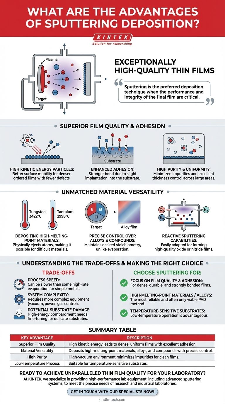
The primary advantage of sputtering deposition is its ability to produce exceptionally high-quality thin films. This method leverages high-energy ion bombardment to eject atoms from a source material, resulting in films with superior adhesion, density, and purity. It offers remarkable versatility, capable of depositing materials with very high melting points, complex alloys, and compounds with precise compositional control.
Sputtering is the preferred deposition technique when the performance and integrity of the final film are critical. It trades the simplicity of other methods for unparalleled control over material properties, making it essential for advanced applications in optics, electronics, and protective coatings.
Superior Film Quality and Adhesion
The defining characteristic of sputtering is the high kinetic energy of the particles being deposited. This fundamental difference from other methods, like thermal evaporation, is the source of its most significant benefits.
The Impact of High Kinetic Energy
In sputtering, atoms are ejected from the target material with significant force. When these atoms arrive at the substrate, they possess much higher kinetic energy than atoms that are simply boiled off in an evaporator.
This energy results in better surface mobility, allowing atoms to settle into a denser, more ordered film structure with fewer defects.
Enhanced Adhesion
The high energy of sputtered atoms creates a stronger bond with the substrate. The arriving particles can slightly implant into the surface, forming a graded interface that dramatically improves film adhesion compared to the gentler deposition from thermal evaporation.
High Purity and Uniformity
Sputtering is a physical vapor deposition (PVD) process typically conducted in a high-vacuum environment. This minimizes the incorporation of impurities from residual gases into the film.
The process also allows for excellent control over film thickness and uniformity across large substrate areas, which is critical for many industrial applications.
Unmatched Material Versatility
Sputtering is not limited by the thermal properties of the source material, opening up a vast range of possibilities that are impossible with other techniques.
Depositing High-Melting-Point Materials
Because sputtering physically ejects atoms rather than melting the source, it can easily deposit materials with extremely high melting points, such as tantalum (2998°C) or tungsten (3422°C). Evaporating these materials is often impractical or impossible.
Precise Control Over Alloys and Compounds
Sputtering excels at depositing complex materials like alloys. The composition of the sputtered film is very close to the composition of the source target, ensuring the desired stoichiometry is maintained. This is difficult to achieve with evaporation, where different elements may evaporate at different rates.
Reactive Sputtering Capabilities
The process can be easily adapted for reactive deposition. By introducing a reactive gas, such as oxygen or nitrogen, into the chamber, it is possible to form high-quality oxide or nitride films (e.g., titanium nitride for hard coatings) directly on the substrate.
Understanding the Trade-offs
While powerful, sputtering is not the universal solution for all deposition needs. Objectivity requires acknowledging its limitations.
Process Speed
While modern magnetron sputtering has significantly increased deposition rates, some high-rate thermal evaporation processes can still be faster for depositing simple metals. The choice often depends on the required film quality versus throughput.
System Complexity and Cost
Sputtering systems are generally more complex and expensive than simple thermal evaporators. They require high-voltage power supplies, robust vacuum systems, and gas flow controllers, which can increase the initial investment and maintenance overhead.
Potential for Substrate Damage
The same high-energy particle bombardment that enhances adhesion can, if not properly controlled, cause damage to extremely delicate substrates like some polymers or organic electronics. Fine-tuning the process parameters is crucial to mitigate this risk.
Making the Right Choice for Your Application
Selecting the correct deposition method depends entirely on your project's specific requirements for film performance, material type, and substrate sensitivity.
- If your primary focus is film quality and adhesion: Sputtering is the definitive choice for creating dense, durable, and strongly bonded films for demanding applications.
- If you are working with high-melting-point materials or complex alloys: Sputtering is the most reliable—and often the only—viable PVD method available.
- If your primary focus is depositing on temperature-sensitive substrates: Sputtering's low-temperature operation gives it a significant advantage over high-temperature methods like Chemical Vapor Deposition (CVD).
- If your primary focus is maximum simplicity and low cost for basic metals: Thermal evaporation may be a more straightforward and economical alternative to consider.
Ultimately, choosing sputtering is an investment in quality, control, and material flexibility.
Summary Table:
| Key Advantage | Description |
|---|---|
| Superior Film Quality | High kinetic energy leads to dense, uniform films with excellent adhesion and fewer defects. |
| Material Versatility | Deposits high-melting-point materials (e.g., Tungsten), alloys, and compounds with precise control. |
| High Purity | High-vacuum environment minimizes impurities, ensuring clean, high-performance films. |
| Low-Temperature Process | Suitable for temperature-sensitive substrates, unlike high-temperature methods like CVD. |
Ready to achieve unparalleled thin film quality for your laboratory?
Sputtering deposition is essential for advanced applications in optics, electronics, and protective coatings where film integrity is critical. At KINTEK, we specialize in providing high-performance lab equipment, including advanced sputtering systems, to meet the precise needs of research and industrial laboratories.
Our experts can help you select the ideal system to deposit everything from simple metals to complex alloys with superior adhesion and purity. Contact us today to discuss your project requirements and discover how KINTEK's solutions can enhance your research and production capabilities.
Get in touch with our specialists now!
Visual Guide
Related Products
- Chemical Vapor Deposition CVD Equipment System Chamber Slide PECVD Tube Furnace with Liquid Gasifier PECVD Machine
- Customer Made Versatile CVD Tube Furnace Chemical Vapor Deposition Chamber System Equipment
- HFCVD Machine System Equipment for Drawing Die Nano-Diamond Coating
- RF PECVD System Radio Frequency Plasma-Enhanced Chemical Vapor Deposition RF PECVD
- 915MHz MPCVD Diamond Machine Microwave Plasma Chemical Vapor Deposition System Reactor
People Also Ask
- What types of substrates are used in CVD to facilitate graphene films? Optimize Graphene Growth with the Right Catalyst
- What happens during deposition chemistry? Building Thin Films from Gaseous Precursors
- What is plasma enhanced chemical vapor deposition PECVD equipment? A Guide to Low-Temperature Thin Film Deposition
- How are carbon nanotubes grown? Master Scalable Production with Chemical Vapor Deposition
- What are the advantages of chemical vapor deposition? Achieve Superior Thin Films for Your Lab


