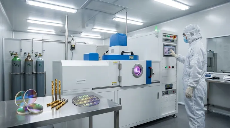
At its core, reactive sputtering is a manufacturing process used to create high-performance compound thin films, such as oxides and nitrides, that cannot be easily made with other methods. Its applications range from depositing anti-reflective optical coatings on lenses to creating ultra-hard, wear-resistant surfaces on cutting tools and producing critical insulating or barrier layers inside microchips.
Reactive sputtering's primary value is its ability to create a complex compound film (like a ceramic) by starting with a simple, pure metallic target. By introducing a reactive gas during the deposition process, you can precisely engineer the final material's chemical composition and properties on the substrate.
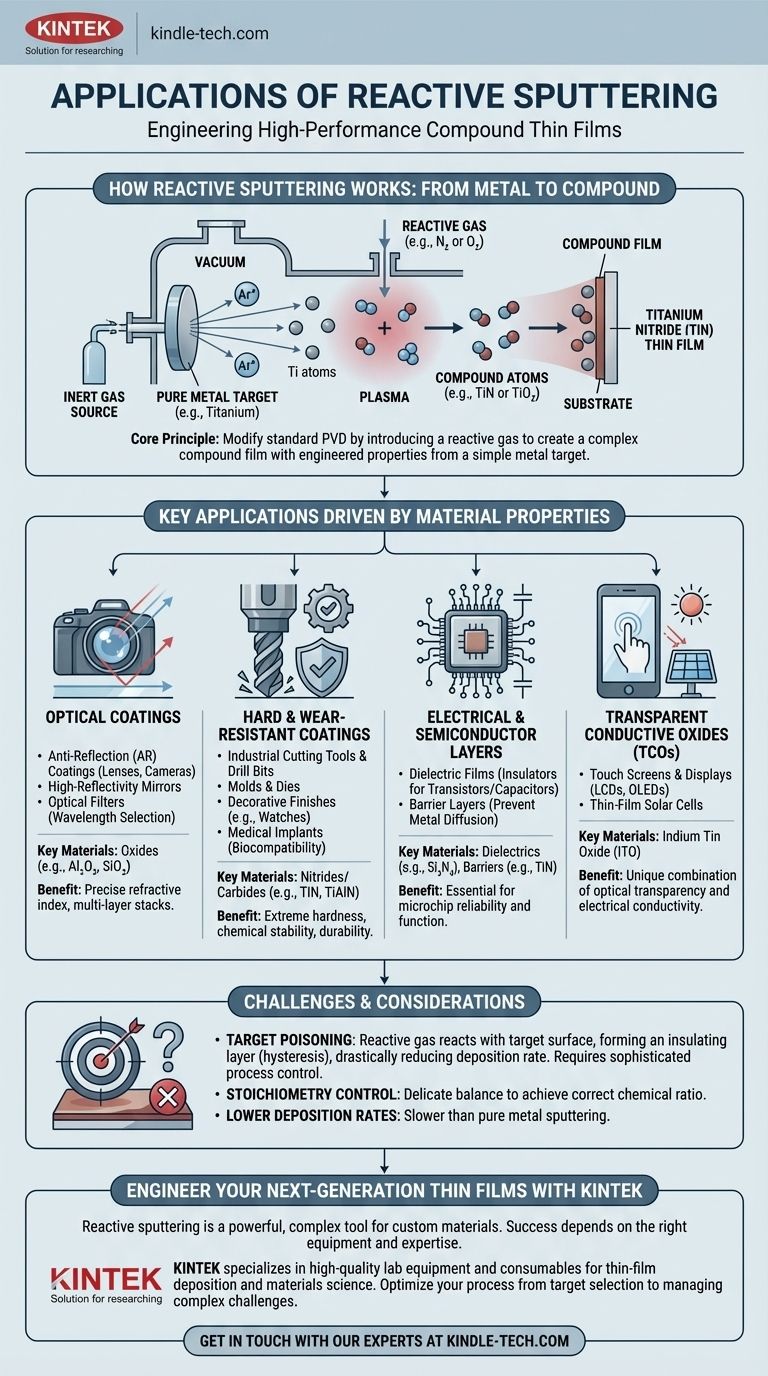
How Reactive Sputtering Works: From Metal to Compound
To understand its applications, you must first understand its fundamental mechanism. It is a modification of a standard Physical Vapor Deposition (PVD) process.
The Basic Sputtering Process
In standard sputtering, a target of the desired material is placed in a vacuum chamber. High-energy ions from an inert gas, typically Argon (Ar), are accelerated into this target, physically knocking off atoms like microscopic billiard balls. These ejected atoms then travel and deposit onto a substrate, forming a thin film.
Introducing the Reactive Gas
Reactive sputtering adds a crucial second step. Along with the inert argon gas, a small, controlled amount of a reactive gas—most commonly Oxygen (O₂) or Nitrogen (N₂)—is introduced into the chamber.
The Chemical Reaction
The atoms ejected from the pure metal target now travel through a plasma rich with this reactive gas. A chemical reaction occurs, transforming the pure metal atoms into a new compound. For example, sputtered titanium (Ti) atoms react with nitrogen to form titanium nitride (TiN).
This reaction can happen in the gas phase on the way to the substrate, or directly on the substrate surface as the film grows.
Deposition of the Compound Film
The final result is that a compound film is deposited onto the substrate, which has a completely different chemical makeup and set of properties than the original metallic target.
Key Applications Driven by Material Properties
The versatility of reactive sputtering comes from the wide range of materials it can produce. The applications are defined by the specific properties of these deposited films.
Optical Coatings
Many oxides, like aluminum oxide (Al₂O₃) or silicon dioxide (SiO₂), are transparent and have a specific refractive index. Reactive sputtering is a dominant method for creating precise, multi-layer optical coatings.
This includes anti-reflection coatings on eyeglass lenses and camera optics, high-reflectivity mirrors, and optical filters that only allow specific wavelengths of light to pass through.
Hard and Wear-Resistant Coatings
Nitrides and carbides, such as titanium nitride (TiN) and titanium aluminum nitride (TiAlN), are exceptionally hard and chemically stable.
These coatings are applied to industrial cutting tools, drill bits, and molds to dramatically increase their lifespan and performance. They are also used for decorative finishes (e.g., a gold-colored TiN on watches) and on medical implants to improve biocompatibility and wear resistance.
Electrical and Semiconductor Layers
Reactive sputtering is critical in microelectronics. It is used to deposit dielectric films (insulators) like silicon nitride (Si₃N₄) and aluminum oxide, which are essential for building transistors and capacitors.
It is also used to create barrier layers, such as TiN, that prevent different metals within the chip's intricate wiring from diffusing into one another and causing a short circuit.
Transparent Conductive Oxides (TCOs)
A special class of materials, like Indium Tin Oxide (ITO), possess the unique combination of being both optically transparent and electrically conductive.
Reactive sputtering is a primary method for depositing TCOs, which are the foundation of modern touch screens, LCDs, OLED displays, and thin-film solar cells.
Understanding the Trade-offs and Challenges
While powerful, reactive sputtering is a complex process with inherent difficulties that must be managed.
The "Target Poisoning" Effect
The biggest challenge is a phenomenon known as hysteresis, or target poisoning. The reactive gas doesn't just react with the sputtered atoms; it also reacts with the surface of the target itself, forming an insulating compound layer.
This "poisoned" layer sputters much more slowly than the pure metal, causing a sudden and dramatic drop in the deposition rate. Managing this instability requires sophisticated process control systems.
Stoichiometry Control
While the process allows for precise control over the film's chemical ratio (stoichiometry), achieving it is a delicate balancing act. A slight drift in gas flow or pressure can result in a film with the wrong composition (e.g., Ti₂O₃ instead of TiO₂), altering its properties.
Lower Deposition Rates
Generally, reactive sputtering is slower than sputtering a pure metallic film. This is partly due to the target poisoning effect and the energy consumed by the chemical reaction itself. For very thick films, this can lead to long processing times.
Making the Right Choice for Your Goal
Reactive sputtering is chosen when the desired film is a compound that is either impossible or impractical to manufacture into a sputter target itself.
- If your primary focus is optical performance: Reactive sputtering is ideal for creating the precise, multi-layer dielectric stacks needed for filters and anti-reflection coatings.
- If your primary focus is mechanical durability: Use this process to deposit hard, inert nitride or carbide coatings for tools, implants, and wear-resistant surfaces.
- If your primary focus is advanced electronics: This is the go-to method for depositing the high-quality insulating, barrier, or transparent conductive films essential for semiconductors and displays.
Ultimately, reactive sputtering empowers engineers and scientists to create custom materials atom-by-atom, building high-performance films from the ground up.
Summary Table:
| Application Area | Key Materials Produced | Primary Benefits |
|---|---|---|
| Optical Coatings | Oxides (e.g., Al₂O₃, SiO₂) | Anti-reflection, precise refractive index, multi-layer filters |
| Hard & Wear-Resistant Coatings | Nitrides/Carbides (e.g., TiN, TiAlN) | Extreme hardness, durability, decorative finishes |
| Electrical & Semiconductor Layers | Dielectrics (e.g., Si₃N₄), Barrier Layers (e.g., TiN) | Insulation, diffusion barriers, microchip reliability |
| Transparent Conductive Oxides (TCOs) | Indium Tin Oxide (ITO) | Optical transparency + electrical conductivity for displays & solar cells |
Ready to Engineer Your Next-Generation Thin Films?
Reactive sputtering is a powerful tool for creating custom compound films with precise properties. Whether you're developing advanced optical systems, durable industrial tools, or cutting-edge semiconductor devices, having the right lab equipment is crucial for success.
KINTEK specializes in high-quality lab equipment and consumables, serving the precise needs of laboratories focused on thin-film deposition and materials science. Our expertise can help you optimize your reactive sputtering process, from selecting the right targets to managing complex challenges like target poisoning.
Contact us today to discuss how our solutions can enhance your research and production capabilities. Let's build the future of materials, together.
Visual Guide
Related Products
- Visual High-Pressure Reactor for In-Situ Observation
- Chemical Vapor Deposition CVD Equipment System Chamber Slide PECVD Tube Furnace with Liquid Gasifier PECVD Machine
- Microwave Plasma Chemical Vapor Deposition MPCVD Machine System Reactor for Lab and Diamond Growth
- Laboratory CVD Boron Doped Diamond Materials
- Inclined Rotary Plasma Enhanced Chemical Vapor Deposition PECVD Equipment Tube Furnace Machine
People Also Ask
- What is the purpose of a high-pressure reactor in oleophilic GO modification? Optimize Grafting and Oil Dispersion.
- How does a high-pressure reactor enhance the adsorption properties of hydrochar? Boost SMS Performance via HTC
- How do high-pressure reactors enhance biochar redox activity? Optimize Surface Functionalization and Energy Density
- How does a high-pressure reactor facilitate reductive amidation? Maximize Yield & Speed in Tandem Reactions
- What role does a high-pressure reactor play in SHS? Achieve Precise Manganese-Doped MAX Phase Synthesis


