At its core, the phenomenon of thin film interference is applied to precisely control how light reflects from a surface. Its most common applications include creating anti-reflective coatings for lenses and solar cells, producing color-selective mirrors and filters for optical instruments, and enabling ultra-precise thickness measurements during the manufacturing of semiconductors.
The central principle is this: by depositing a transparent layer of a specific, controlled thickness onto a surface, you can dictate which wavelengths (colors) of light are canceled out and which are reinforced, effectively sculpting the light that reflects from it.
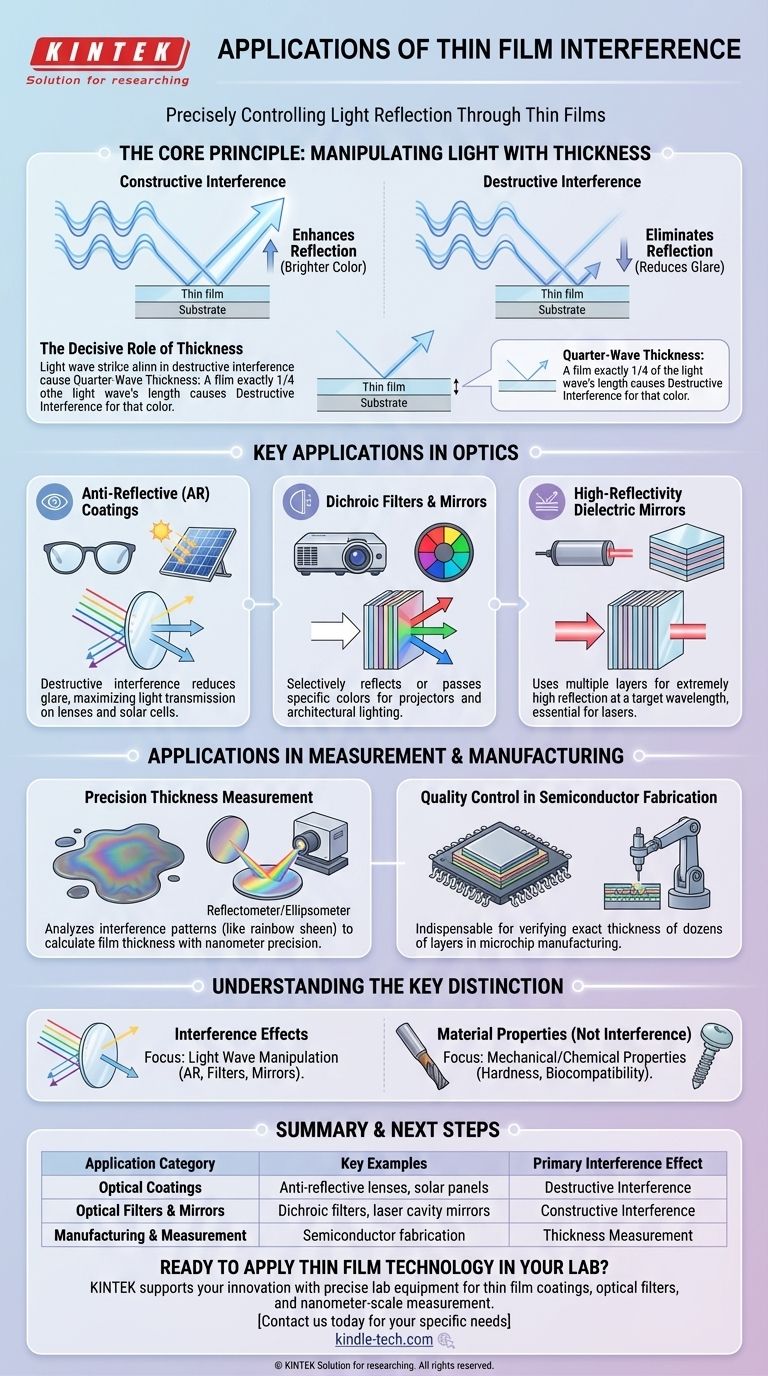
The Core Principle: Manipulating Light with Thickness
Thin film interference arises when light waves reflecting from the top surface of a thin film interact with light waves reflecting from the bottom surface.
Constructive vs. Destructive Interference
When these two sets of reflected light waves align, their crests and troughs match up. This is called constructive interference, and it makes that specific color of light appear brighter.
If the waves are out of sync—the crest of one wave aligns with the trough of another—they cancel each other out. This is destructive interference, which eliminates or dramatically reduces the reflection of that specific color.
The Decisive Role of Thickness
The outcome—constructive or destructive interference—depends entirely on the thickness of the film relative to the wavelength of the light.
A film that is exactly one-quarter of a light wave's length will cause destructive interference for that specific color. By precisely controlling the film's thickness during manufacturing, we can choose exactly which colors to eliminate or enhance.
Key Applications in Optics
This ability to manipulate light is the foundation for numerous optical technologies. These applications rely directly on the interference effect.
Anti-Reflective (AR) Coatings
This is the most widespread application. By applying a thin coating (like magnesium fluoride) to a lens or solar panel, manufacturers tune the thickness to cause destructive interference for wavelengths in the middle of the visible spectrum.
This cancels out reflections, reducing glare and allowing more light to pass through. You find this on eyeglasses, camera lenses, and the glass covering solar cells to maximize energy capture.
Dichroic Filters and Mirrors
These are optical filters that selectively pass certain colors while reflecting others. This is achieved by using one or more thin film layers tuned for constructive interference for the colors to be reflected.
This technology is critical in digital projectors to separate red, green, and blue light and in architectural and stage lighting to produce pure, saturated colors without using inefficient gels.
High-Reflectivity Dielectric Mirrors
While a normal mirror reflects a broad spectrum of light, a dielectric mirror (or Bragg reflector) uses multiple stacked thin films to create extremely high reflectivity for a very narrow range of wavelengths.
Each layer is designed for constructive interference at the target wavelength. This is essential for building laser cavities, where near-perfect reflection is required to sustain laser operation.
Applications in Measurement and Manufacturing
Beyond manipulating light, the interference pattern itself is a powerful diagnostic tool.
Precision Thickness Measurement
The colors produced by thin film interference (like the rainbow sheen on an oil slick) are a direct indicator of the film's thickness. Automated instruments called reflectometers or ellipsometers shine light on a film and analyze the reflected spectrum.
By observing which wavelengths are enhanced or canceled, these tools can calculate the film's thickness with nanometer-level precision.
Quality Control in Semiconductor Fabrication
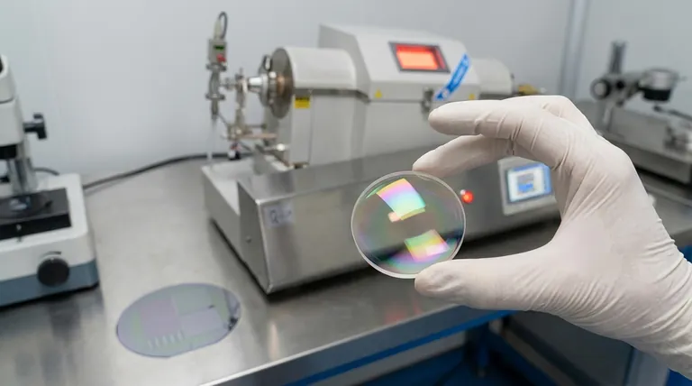
This measurement technique is indispensable in the semiconductor industry. Manufacturing a microchip involves depositing dozens of thin layers of materials like silicon oxide and silicon nitride onto a wafer.
The function of the final transistor depends on these layers having the exact specified thickness. Thin film interference is the primary method used to verify this at every step, ensuring the reliability and performance of the chip.
Understanding the Key Distinction
It is critical to separate the applications of thin film interference from the broader applications of thin films as a material science technology.
Interference Effects vs. Material Properties
Many thin film applications do not use interference. For example, depositing a hard, diamond-like carbon (DLC) coating on a cutting tool is done for its mechanical properties (hardness and low friction), not its optical effects.
Similarly, thin films on medical implants improve biocompatibility or enable drug delivery. These are chemical and material properties, distinct from the wave interference of light.
Manufacturing Complexity
Creating films with the precise thickness and uniformity required for optical interference effects is a complex and expensive process. It requires high-vacuum deposition equipment (like PVD or CVD systems) and stringent quality control, which adds to the cost of the final product.
Applying This Principle to Your Goal
Understanding the core mechanism allows you to identify the right application for your objective.
- If your primary focus is maximizing light transmission or reducing glare: The solution is an anti-reflective coating designed for destructive interference.
- If your primary focus is separating or reflecting specific colors: The solution is a dichroic filter or dielectric mirror designed for constructive interference at target wavelengths.
- If your primary focus is manufacturing and process control: The solution is to use the interference pattern itself as a measurement tool for ensuring nanometer-scale accuracy.
By mastering this fundamental principle of wave physics, we enable some of our most advanced optical and electronic technologies.
Summary Table:
| Application Category | Key Examples | Primary Interference Effect |
|---|---|---|
| Optical Coatings | Anti-reflective lenses, solar panels | Destructive Interference (reduces reflection) |
| Optical Filters & Mirrors | Dichroic filters, laser cavity mirrors | Constructive Interference (enhances reflection) |
| Manufacturing & Measurement | Semiconductor fabrication, quality control | Thickness Measurement via interference pattern |
Ready to Apply Thin Film Technology in Your Lab?
KINTEK specializes in the precise lab equipment and consumables needed to develop and apply thin film coatings. Whether you are creating anti-reflective surfaces, advanced optical filters, or require nanometer-scale measurement tools, our expertise supports your innovation in optics and semiconductor manufacturing.
Contact us today to discuss your specific needs and discover how KINTEK can enhance your laboratory's capabilities.
Visual Guide
Related Products
People Also Ask
- For what types of systems, temperature ranges, and sealing configurations is the thin-layer spectroelectrochemical cell designed? Ideal for Aqueous and Non-Aqueous Analysis
- What are the general operating procedures for a thin-layer spectroelectrochemical cell during an experiment? Master Synchronized Data Collection
- What are the physical dimensions of the thin-layer spectroelectrochemical cell body and its slit? Key Specs for Your Lab
- What are the necessary preparation steps before using a thin-layer spectroelectrochemical cell? A Guide to Reliable Results
- What operational environments and sealing options are available for the thin-layer spectroelectrochemical cell?
