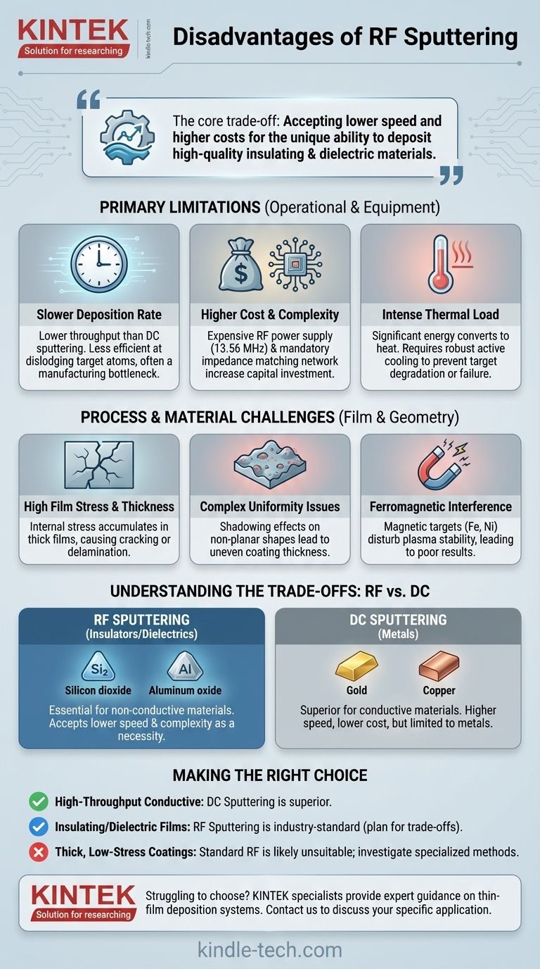
The primary disadvantages of RF sputtering are its significantly lower deposition rates, higher system cost and complexity, and challenges in producing thick, low-stress films. Unlike the simpler Direct Current (DC) method, Radio Frequency (RF) sputtering requires an expensive power supply and an impedance matching network, making the entire process slower and more capital-intensive.
The core trade-off of RF sputtering is accepting lower speed and higher costs in exchange for the unique ability to deposit high-quality insulating and dielectric materials, a task that simpler methods like DC sputtering cannot perform.
The Primary Limitations of RF Sputtering
While versatile, the RF sputtering process comes with inherent drawbacks related to its operational physics and equipment requirements.
Deposition Rate
The most frequently cited disadvantage is the slow deposition rate. Compared to DC sputtering for conductive materials, RF sputtering is fundamentally less efficient at dislodging target atoms for a given power input.
While adding magnets (RF magnetron sputtering) can improve the rate by trapping electrons, it often remains a bottleneck for high-throughput manufacturing.
Cost and System Complexity
RF sputtering systems are significantly more expensive and complex than their DC counterparts. This is driven by two key components.
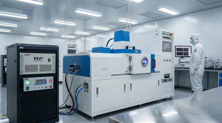
First is the RF power supply, which operates at a federally regulated frequency (typically 13.56 MHz) and is more costly to manufacture. Second is the required impedance matching network, a critical and complex device that ensures maximum power is transferred from the supply to the plasma, preventing power reflection that could damage the equipment.
Thermal Management
A large portion of the energy applied to the sputtering target is converted into heat rather than kinetic energy for sputtering atoms. This intense thermal load must be actively removed with a robust cooling system.
Inefficient cooling can lead to target degradation, inconsistent deposition rates, and even catastrophic failure of the target bonding.
Process and Material-Specific Challenges
Beyond the primary limitations, several challenges arise during the deposition process itself, especially with certain materials or film requirements.
Film Stress and Thickness
RF-sputtered films often exhibit high internal residual stress. While manageable for thin coatings, this stress accumulates as the film gets thicker.
This makes it very difficult to produce thick, high-performance coatings without issues like cracking, peeling, or delamination from the substrate.
Uniformity on Complex Geometries
Achieving a perfectly uniform coating on substrates with complex, non-planar shapes is a significant challenge. The directional nature of the sputtering process can lead to shadowing effects, causing thicker films on surfaces facing the target and thinner films on others.
Issues with Ferromagnetic Targets
When sputtering magnetic materials like iron or nickel, the target's own magnetic field can interfere with the RF process and any magnetron confinement. This can disturb the plasma, leading to process instability and poor deposition results.
Understanding the Trade-offs: RF vs. DC Sputtering
The disadvantages of RF sputtering are best understood in the context of its primary alternative, DC sputtering. The choice between them is almost always dictated by the target material.
The Core Difference: Target Material
DC sputtering can only be used for conductive materials (metals). If a direct current is applied to an insulating target, positive charge builds up on its surface, effectively stopping the sputtering process almost immediately.
RF sputtering solves this by using an AC field. The rapid oscillation of voltage prevents charge accumulation, making it the essential technique for depositing insulating and dielectric materials like silicon dioxide (SiO₂) or aluminum oxide (Al₂O₃).
Speed vs. Versatility
This creates a clear decision point. DC sputtering is the superior choice for metals due to its higher speed and lower cost. RF sputtering is the necessary choice for insulators, and its associated disadvantages are accepted as a required trade-off for its material versatility.
Making the Right Choice for Your Application
Selecting the correct sputtering technique requires aligning the process capabilities with your primary goal.
- If your primary focus is high-throughput deposition of conductive materials: DC magnetron sputtering is the clear choice for its superior speed and lower operational cost.
- If your primary focus is depositing insulating or dielectric films: RF sputtering is the industry-standard solution, and you must plan for the inherent trade-offs in speed and system complexity.
- If your primary focus is creating thick, low-stress coatings: Standard RF sputtering is likely unsuitable; you should investigate specialized low-stress deposition techniques or other methods entirely.
Ultimately, understanding these limitations allows you to choose the right deposition tool for your specific material and performance requirements.
Summary Table:
| Disadvantage | Key Impact |
|---|---|
| Slower Deposition Rate | Lower throughput compared to DC sputtering for metals. |
| Higher Cost & Complexity | Expensive RF power supply and impedance matching network required. |
| High Film Stress | Difficult to produce thick coatings without cracking or delamination. |
| Thermal Management | Requires robust cooling to prevent target damage from heat buildup. |
Struggling to choose the right sputtering technique for your insulating or dielectric materials? KINTEK specializes in lab equipment and consumables, serving laboratory needs with expert guidance on thin-film deposition systems. Let our specialists help you navigate the trade-offs and select the optimal solution for your research or production goals. Contact us today to discuss your specific application and unlock the full potential of your lab!
Visual Guide
Related Products
- RF PECVD System Radio Frequency Plasma-Enhanced Chemical Vapor Deposition RF PECVD
- Spark Plasma Sintering Furnace SPS Furnace
- Horizontal High Temperature Graphite Vacuum Graphitization Furnace
People Also Ask
- What is plasma enhanced chemical vapour deposition process? Unlock Low-Temperature, High-Quality Thin Films
- What is plasma enhanced chemical vapour deposition PECVD used for? Enable Low-Temp Thin Films for Electronics & Solar
- Why is a Matching Network Indispensable in RF-PECVD for Siloxane Films? Ensure Stable Plasma and Uniform Deposition
- What is plasma chemical vapor deposition? A Low-Temperature Thin Film Coating Solution
- What is plasma CVD? Unlock Low-Temperature Thin Film Deposition for Sensitive Materials


