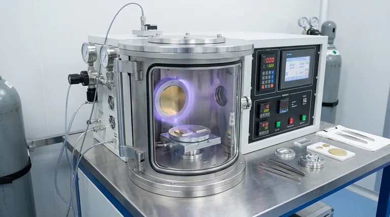
In essence, a sputter coater is a high-vacuum instrument used to deposit an exceptionally thin, uniform layer of a material onto a surface. It operates not through a chemical reaction or melting, but through a physical process where high-energy ions bombard a source material (the "target"), physically knocking atoms loose, which then deposit onto the desired object (the "substrate").
A sputter coater is best understood as a subatomic sandblaster. It uses energetic gas ions to precisely chip atoms off a source material and deposit them as a highly controlled thin film, making it indispensable for applications requiring precision coatings, from microelectronics to preparing samples for powerful microscopes.
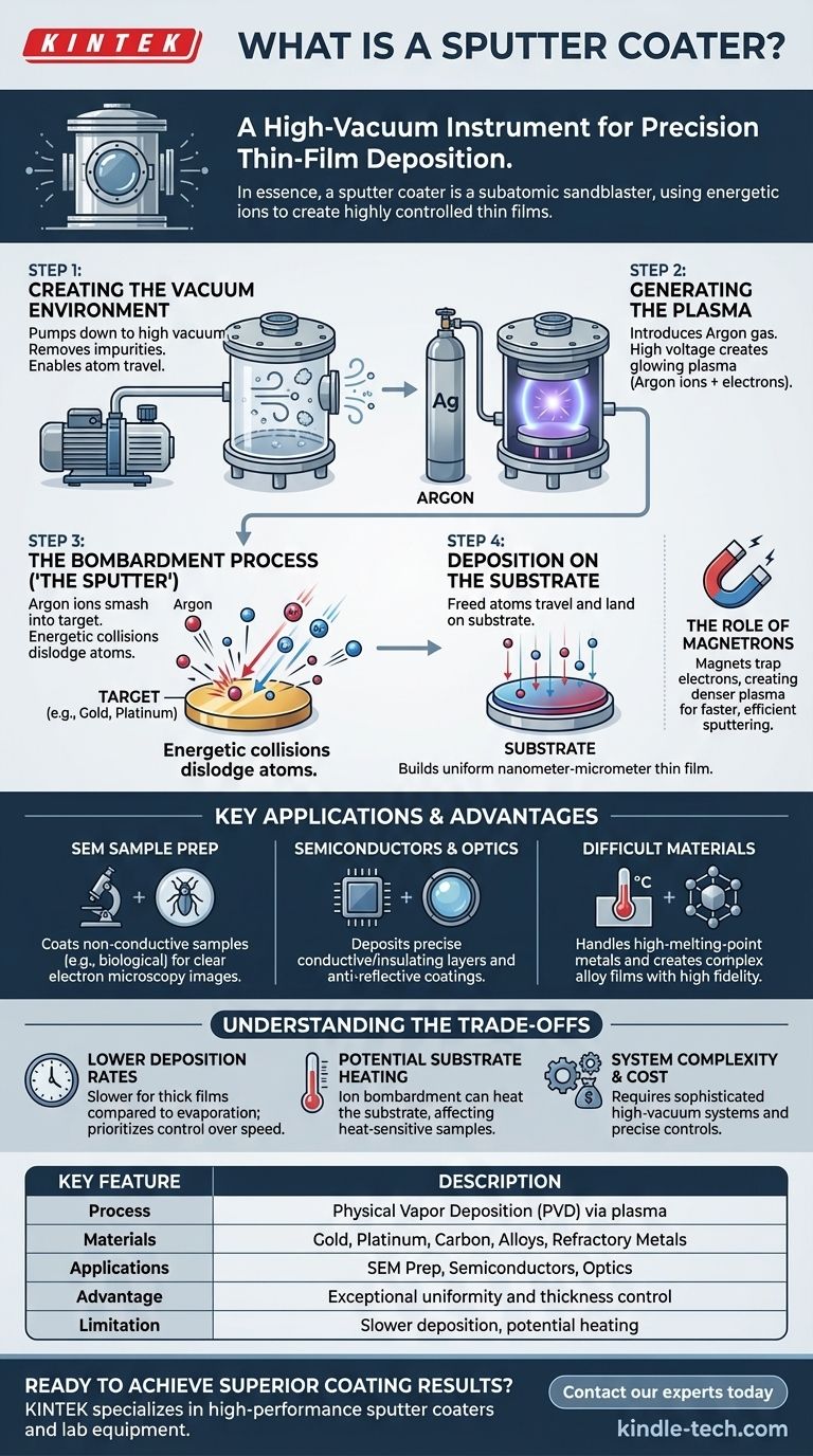
How Sputtering Achieves Precision Coating
The entire process occurs within a high-vacuum chamber, which is critical for ensuring the purity and quality of the final film. Each step is precisely controlled to achieve a specific thickness and morphology.
Step 1: Creating the Vacuum Environment
Before any coating can begin, the chamber is pumped down to a high vacuum. This serves two purposes: it removes atmospheric gases that could contaminate the coating, and it allows the sputtered atoms to travel from the target to the substrate without colliding with other particles.
Step 2: Generating the Plasma
A small, controlled amount of an inert gas, almost always argon, is introduced into the chamber. A high voltage is then applied between the target material (acting as a cathode) and the chamber. This electrical field energizes the argon gas, stripping electrons from the argon atoms and creating a glowing plasma—a mixture of positively charged argon ions and free electrons.
Step 3: The Bombardment Process (The "Sputter")
The positively charged argon ions are accelerated by the electric field and smash into the negatively charged target material (e.g., a disc of gold, platinum, or carbon). This energetic collision has enough force to dislodge, or "sputter," individual atoms from the target's surface.
Step 4: Deposition on the Substrate
These newly freed atoms from the target travel in straight lines through the vacuum and land on the surface of the sample, or substrate, which is positioned nearby. Atom by atom, they build up to form an extremely thin and uniform film, with thicknesses ranging from just a few nanometers to several micrometers.
The Role of Magnetrons
Many modern systems are magnetron sputter coaters. They use powerful magnets behind the target to trap electrons in a magnetic field close to the target's surface. This dramatically increases the probability of electrons colliding with argon atoms, creating a denser plasma and accelerating the sputtering process, making it far more efficient.
Key Applications and Advantages
Sputtering is not just one deposition method among many; it has specific advantages that make it the ideal choice for demanding applications.
Preparing Samples for Electron Microscopy
One of the most common uses is preparing non-conductive samples (like insects, ceramics, or polymers) for a Scanning Electron Microscope (SEM). An SEM requires the sample to be electrically conductive. Sputtering a thin layer of a metal like gold or platinum prevents charge buildup and allows for a clear, high-resolution image.
Fabricating Semiconductors and Optics
The process is a cornerstone of the semiconductor industry. It is used to deposit the precise layers of conductive or insulating materials required to build microchips. It is also used to apply anti-reflective or reflective coatings on optical lenses and other devices.
Handling Difficult Materials
Sputtering excels where other methods, like simple thermal evaporation, fall short. It can be used to deposit materials with extremely high melting points (refractory metals) and to create films of complex alloys while preserving their original composition, as the target is sputtered away layer by layer.
Understanding the Trade-offs
While powerful, sputtering is not a universal solution. Understanding its limitations is key to using it effectively.
Lower Deposition Rates
Compared to a process like thermal evaporation, sputtering can be a slower method for building up thick films. Its strength lies in control and uniformity, not speed.
Potential for Substrate Heating
The constant bombardment of energetic particles (argon ions, electrons, and sputtered atoms) transfers energy to the substrate, causing it to heat up. This can be a significant problem for heat-sensitive substrates, such as biological specimens or certain polymers.
System Complexity and Cost
Sputter coaters are sophisticated instruments that require a high-vacuum system, high-voltage power supplies, and precise gas flow controllers. This complexity translates to higher initial cost and maintenance requirements compared to simpler coating techniques.
How to Apply This to Your Project
Your choice of a deposition technique depends entirely on your end goal. Sputtering is a tool for precision and control.
- If your primary focus is preparing non-conductive samples for SEM: Sputtering is the industry-standard method and the right choice for achieving a thin, uniform, conductive coating.
- If your primary focus is fabricating devices with complex, thin-film layers: Sputtering offers the precise thickness control and material fidelity required for semiconductors, sensors, and advanced optics.
- If your primary focus is depositing alloys or high-melting-point metals: Sputtering is often the most reliable, and sometimes the only, viable physical vapor deposition technique.
By understanding sputtering as a controlled physical bombardment process, you can effectively leverage its capabilities for creating high-quality, functional thin films.
Summary Table:
| Key Feature | Description |
|---|---|
| Process | Physical Vapor Deposition (PVD) via plasma bombardment |
| Typical Coating Materials | Gold, Platinum, Carbon, Alloys, Refractory Metals |
| Primary Applications | SEM Sample Preparation, Semiconductor Fabrication, Optical Coatings |
| Key Advantage | Exceptional uniformity and control over film thickness and composition |
| Main Limitation | Slower deposition rates and potential for substrate heating |
Ready to achieve superior coating results?
KINTEK specializes in high-performance sputter coaters and lab equipment designed to meet the precise demands of researchers and engineers. Whether you are preparing samples for electron microscopy or developing next-generation thin-film devices, our solutions deliver the reliability and control you need.
Contact our experts today to discuss how our sputtering technology can enhance your laboratory's capabilities and accelerate your project's success.
Visual Guide
Related Products
- Custom CVD Diamond Coating for Lab Applications
- HFCVD Machine System Equipment for Drawing Die Nano-Diamond Coating
- Chemical Vapor Deposition CVD Equipment System Chamber Slide PECVD Tube Furnace with Liquid Gasifier PECVD Machine
- Multifunctional Electrolytic Electrochemical Cell Water Bath Single Layer Double Layer
- Professional Cutting Tools for Carbon Paper Cloth Diaphragm Copper Aluminum Foil and More
People Also Ask
- What is CVD coated? A Guide to Superior Wear Resistance for Complex Parts
- What is CVD diamond coating? Grow a Super-Hard, High-Performance Diamond Layer
- What are the advantages of CVD coating? Superior Hardness and Uniformity for Demanding Applications
- Can you coat something in diamond? Unlock Unmatched Hardness and Thermal Conductivity
- What are the different CVD coating? A Guide to Thermal CVD, PECVD, and Specialized Methods


