In short, sputter coating is used to apply exceptionally thin, uniform, and durable films of material onto a surface. This process is critical for manufacturing high-performance products, including electronic circuits, optical lenses, energy-efficient glass, and wear-resistant tools. It functions at a near-atomic level to build films with precisely controlled thickness and composition.
The core reason sputter coating is chosen over other methods is its ability to produce highly dense and strongly bonded films with unparalleled uniformity, even over large areas. This control makes it indispensable for applications where film quality and reliability are more important than raw deposition speed.

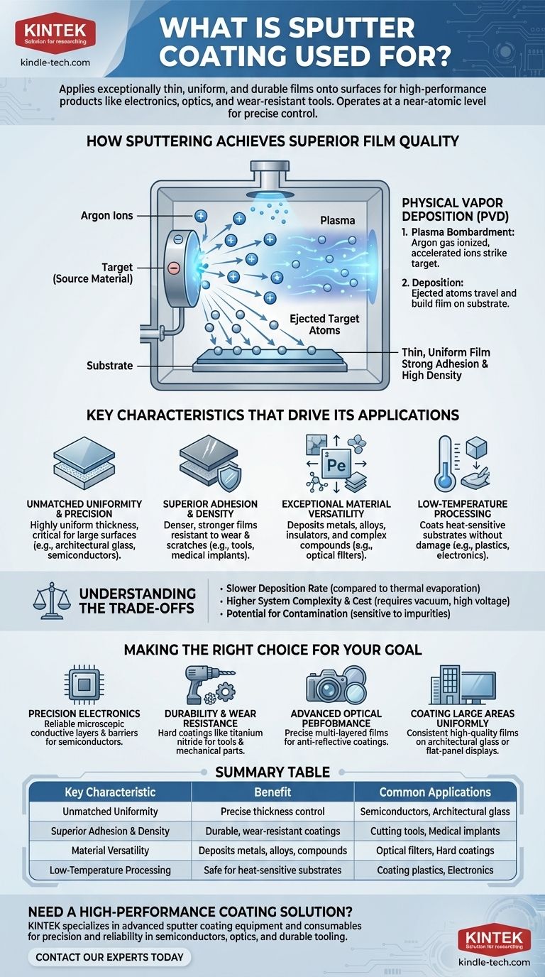
How Sputtering Achieves Superior Film Quality
Sputter coating is a physical vapor deposition (PVD) method that works by ejecting atoms from a source material (called a "target") and depositing them onto another material (the "substrate"). The mechanism behind this process is what gives the resulting film its superior characteristics.
The Core Principle: Plasma Bombardment
The process begins inside a vacuum chamber. A gas, typically argon, is introduced and energized to create a plasma—a state of matter containing positive ions and free electrons.
A high voltage is applied to the target, giving it a negative charge. This attracts the positive argon ions from the plasma, which accelerate and collide with the target's surface with significant force.
This atomic-scale bombardment is energetic enough to knock atoms loose from the target material. These ejected atoms then travel through the vacuum chamber.
Deposition: Building the Film Atom by Atom
The ejected target atoms travel until they strike the substrate, which is strategically placed nearby. Upon impact, they stick and gradually build up to form a thin, solid film.
Because the atoms are ejected with high kinetic energy, they embed themselves slightly into the substrate and pack together very tightly. This is why sputtered films are known for their strong adhesion and high density.
Key Characteristics That Drive Its Applications
The unique properties of the sputtering process directly translate into benefits that are essential for modern technology. Understanding these characteristics shows why it is the preferred method in so many advanced fields.
Unmatched Uniformity and Precision
The stable plasma created during sputtering ensures an even and consistent rate of atom ejection from the target. This results in a film of highly uniform thickness, which is critical for coating large surfaces like architectural glass or for creating predictable electrical properties in semiconductors. Film thickness can be controlled with extreme precision by managing the process time and power.
Superior Adhesion and Density
Compared to other methods like thermal evaporation (which essentially boils a material), sputtering produces films that are denser and adhere much more strongly to the substrate. This makes the coating far more durable and resistant to scratches and wear, a vital feature for cutting tools and medical implants.
Exceptional Material Versatility
Sputtering is not limited to pure metals. It can be used to deposit alloys, insulators, and complex compounds. By introducing a reactive gas like oxygen or nitrogen into the vacuum chamber, it's possible to form oxide or nitride films (e.g., titanium nitride) directly on the substrate, creating coatings with specific hard, optical, or dielectric properties.
Low-Temperature Processing
While the plasma bombardment involves high energy, the overall process can be managed at relatively low temperatures. This allows for coating heat-sensitive substrates, such as plastics and pre-existing electronic components, without causing damage.
Understanding the Trade-offs
No process is perfect for every scenario. Being an effective advisor means acknowledging the limitations of sputter coating.
Slower Deposition Rate
Generally, sputtering deposits material more slowly than thermal evaporation methods. For applications where film quality is secondary to speed and cost, other methods might be more economical.
Higher System Complexity and Cost
Sputter coating systems require a vacuum chamber, high-voltage power supplies, and gas control systems. This equipment is more complex and expensive to acquire and maintain than simpler coating technologies.
Potential for Contamination
Because the process is so precise, it is also highly sensitive to impurities within the vacuum chamber. Any unwanted molecules can become incorporated into the film, altering its properties. This necessitates a meticulously clean environment.
Making the Right Choice for Your Goal
Ultimately, the decision to use sputter coating is driven by the performance requirements of the final product.
- If your primary focus is precision electronics: Sputtering is the standard for creating the reliable, microscopic conductive layers and barrier films essential for modern semiconductors.
- If your primary focus is durability and wear resistance: Sputtering hard materials like titanium nitride provides a dense, strongly adhered film ideal for extending the life of tools and mechanical parts.
- If your primary focus is advanced optical performance: The process allows for the precise, multi-layered films required for anti-reflective coatings on lenses and selective filters on glass.
- If your primary focus is coating large areas uniformly: Sputtering is one of the few methods that can deliver a consistent, high-quality film on products like architectural glass or flat-panel displays.
By understanding these core principles, you can recognize when sputter coating is not just an option, but the necessary choice for achieving superior material performance.
Summary Table:
| Key Characteristic | Benefit | Common Applications |
|---|---|---|
| Unmatched Uniformity | Precise thickness control | Semiconductors, architectural glass |
| Superior Adhesion & Density | Durable, wear-resistant coatings | Cutting tools, medical implants |
| Material Versatility | Deposits metals, alloys, compounds | Optical filters, hard coatings |
| Low-Temperature Processing | Safe for heat-sensitive substrates | Coating plastics, electronics |
Need a high-performance coating solution for your lab or production line? KINTEK specializes in advanced sputter coating equipment and consumables, delivering the precision and reliability required for semiconductors, optics, and durable tooling. Contact our experts today to discuss how our solutions can enhance your product performance and durability.
Visual Guide
Related Products
- Infrared Transmission Coating Sapphire Sheet Substrate Window
- Electron Beam Evaporation Coating Oxygen-Free Copper Crucible and Evaporation Boat
- 400-700nm Wavelength Anti Reflective AR Coating Glass
- Custom CVD Diamond Coating for Lab Applications
- Molybdenum Tungsten Tantalum Special Shape Evaporation Boat
People Also Ask
- How can we create a reducing environment? Master the Methods for Precise Chemical Control
- What are the applications of optical coating? Unlock Advanced Light Control for Your Industry
- Why do we need optical coating? To Control Light and Enhance Optical Performance
- What is optical coating used for? Control Light for Enhanced Performance in Your Applications
- Is Sputter Tint good? Premium Heat Rejection & Long-Term Durability Explained


