In advanced manufacturing and materials science, a sputtered film is an ultra-thin layer of material deposited onto a surface atom-by-atom using a process called sputter deposition. This technique is a type of Physical Vapor Deposition (PVD) where atoms are physically ejected from a source material (a "target") inside a vacuum and then condense onto a substrate, forming a film of exceptional purity, density, and adhesion.
Sputtering is not merely a coating method; it is a foundational process for engineering materials at the atomic level. By using high-energy ions to physically dislodge atoms from a source, it creates films with superior adhesion and structural integrity that are often impossible to achieve with simple evaporation or chemical methods.
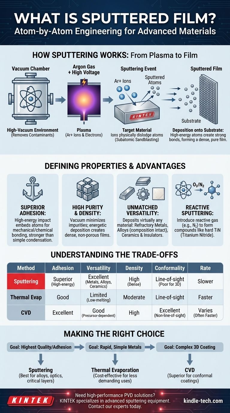
How Sputtering Works: From Plasma to Film
Sputtering is a highly controlled process that takes place within a vacuum chamber. Understanding the sequence of events reveals why the resulting films have such unique properties.
The Vacuum Environment
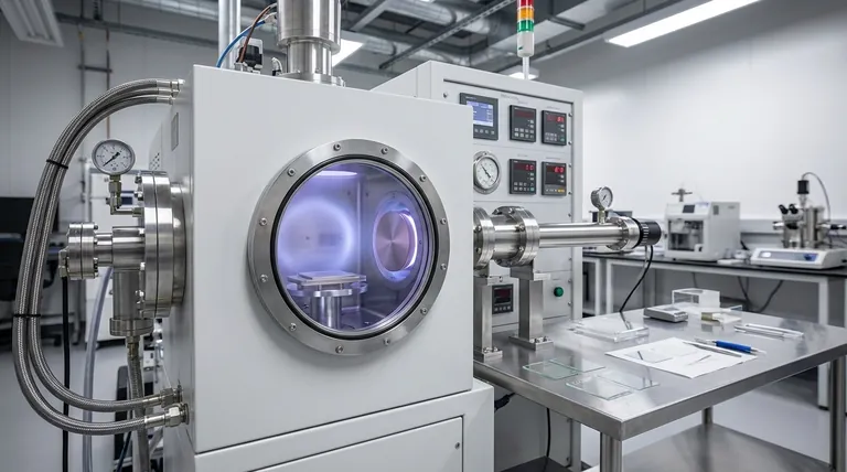
First, a substrate (the object to be coated) and a target (the source material for the film) are placed in a high-vacuum chamber. This vacuum is critical as it removes atmospheric gases that could otherwise contaminate the film or interfere with the process.
Creating the Plasma
An inert gas, most commonly argon, is introduced into the chamber at low pressure. A high voltage is then applied, which ionizes the argon gas and creates a glowing, energetic state of matter known as plasma.
The "Sputtering" Event
The plasma consists of positive argon ions and free electrons. The positively charged ions are accelerated by an electric field and bombard the surface of the target, which is held at a negative potential. This collision is like a subatomic sandblasting, where the impact energy is high enough to physically knock out, or "sputter," individual atoms from the target material.
Deposition onto the Substrate
These sputtered atoms travel through the vacuum chamber and land on the substrate. As they accumulate, they form a thin, highly uniform, and dense film. Because the atoms arrive with significant kinetic energy, they bond very strongly to the substrate surface.
The Defining Properties of a Sputtered Film
The "how" of sputtering directly leads to the "why" it is used. The properties of sputtered films make them essential for high-performance applications.
Superior Adhesion
Sputtered atoms impact the substrate with high energy, which can embed them slightly into the surface. This creates a much stronger mechanical and chemical bond than methods where atoms simply condense with low energy, like thermal evaporation.
High Purity and Density
The high-vacuum environment minimizes impurities, and the energetic deposition process packs the atoms together tightly. This results in dense, non-porous films with predictable electrical and optical properties.
Unmatched Material Versatility
Unlike thermal evaporation, which is limited to materials that can be melted and boiled, sputtering can deposit virtually any material. This includes refractory metals with extremely high melting points (like tungsten or tantalum), alloys (which deposit with their original composition intact), and even ceramics and insulators.
Reactive Sputtering for Compounds
By introducing a reactive gas like oxygen or nitrogen into the chamber along with argon, one can form compound films. For example, sputtering a titanium target in a nitrogen environment creates an exceptionally hard, gold-colored titanium nitride (TiN) film directly on the substrate.
Understanding the Trade-offs
Sputtering is a powerful technique, but it is not the only option for thin film deposition. Its advantages must be weighed against its limitations and compared to other common methods.
Sputtering vs. Thermal Evaporation
Thermal evaporation, another PVD method, involves heating a material until it evaporates and condenses on a substrate. While often faster and simpler for pure metals, its films typically have lower adhesion and density than sputtered films. Sputtering is far superior for alloys and high-melting-point materials.
Sputtering vs. Chemical Vapor Deposition (CVD)
CVD uses chemical reactions of precursor gases to grow a film on a heated substrate. A key advantage of CVD is its ability to produce highly conformal coatings that uniformly cover complex, three-dimensional shapes. Sputtering, being a line-of-sight process, struggles with coating hidden surfaces or deep trenches.
The Challenge of Deposition Rates
A primary trade-off with sputtering is its deposition rate, which is often lower than that of thermal evaporation or certain CVD processes. This can make it a slower and more expensive option for applications where maximum film quality is not the overriding concern.
Making the Right Choice for Your Goal
Selecting a deposition method requires aligning the process capabilities with the end-use requirements of the film.
- If your primary focus is the highest possible film quality and adhesion: Sputtering is the definitive choice, especially for alloys, compounds, and critical optical or electronic layers.
- If your primary focus is rapid deposition of simple metals: Thermal evaporation often provides a more cost-effective and faster solution for less demanding applications.
- If your primary focus is uniformly coating a complex 3D object: Chemical Vapor Deposition (CVD) is generally the superior method due to its non-line-of-sight nature.
Ultimately, mastering sputtering allows engineers and scientists to precisely control the fundamental properties of materials, building high-performance devices from the atom up.
Summary Table:
| Property | Sputtered Film | Thermal Evaporation | Chemical Vapor Deposition (CVD) |
|---|---|---|---|
| Adhesion | Superior (High-energy impact) | Good | Excellent |
| Material Versatility | Excellent (Metals, Alloys, Ceramics) | Limited (Low-melting-point materials) | Good (Depends on precursors) |
| Film Density/Purity | High (Dense, non-porous) | Moderate | High |
| Coating Conformality | Line-of-sight (Poor for complex shapes) | Line-of-sight | Excellent (Non-line-of-sight) |
| Deposition Rate | Slower | Faster | Varies (Often faster) |
Need to deposit high-performance thin films for your laboratory or production line? KINTEK specializes in advanced lab equipment and consumables for sputtering and other Physical Vapor Deposition (PVD) processes. Our expertise can help you achieve the superior adhesion, purity, and material versatility required for your most demanding applications in electronics, optics, and advanced materials. Contact our experts today to discuss your specific thin film requirements and find the ideal solution for your laboratory needs.
Visual Guide
Related Products
- Lab Blown Film Extrusion Three Layer Co-Extrusion Film Blowing Machine
- Tungsten Evaporation Boat for Thin Film Deposition
- Aluminum-Plastic Flexible Packaging Film for Lithium Battery Packaging
People Also Ask
- What is the blown film extrusion technique? Mastering Biaxial Orientation for Superior Film Strength
- What is the blown film extrusion method? Master the Art of Strong, Seamless Plastic Film Production
- What are the advantages of blown film extrusion? Boost Your Film Production Efficiency
- What are the disadvantages of blown film extrusion? Overcoming Precision and Speed Limitations
- What does a blown film machine do? Transform Plastic Pellets into Versatile Film


