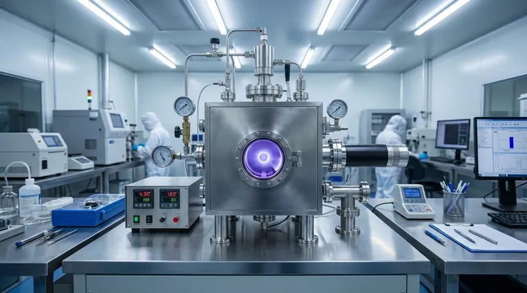
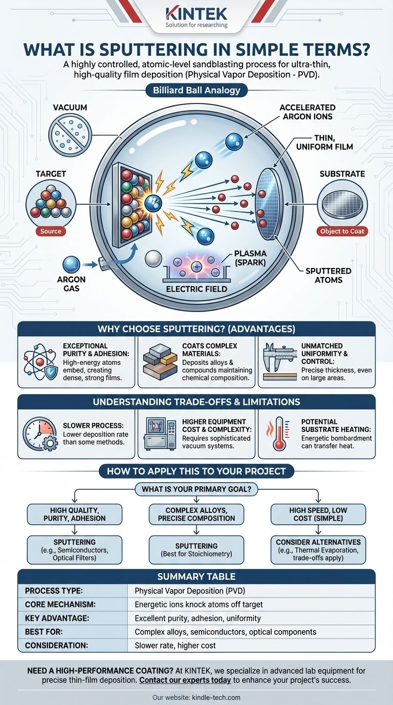
At its core, sputtering is a highly controlled, atomic-level sandblasting process. It uses energized particles to physically knock atoms off a source material, which then fly across a vacuum and deposit as an ultra-thin, high-quality film onto a target surface. This method is not chemical; it relies purely on the kinetic energy of physical collisions.
Sputtering is a type of Physical Vapor Deposition (PVD) where you bombard a source material (the "target") with energetic ions in a vacuum. This bombardment ejects atoms from the target, which then condense on a nearby object (the "substrate") to form a precise and durable coating.
How Sputtering Works: The Billiard Ball Analogy
To understand sputtering, it's helpful to visualize a game of atomic-scale pool. The entire process takes place inside a sealed vacuum chamber.
The Setup: A Vacuum Chamber
First, almost all the air is pumped out of a chamber. This vacuum is critical because it ensures the atoms traveling from the source to the target don't collide with air molecules, which would disrupt the process and contaminate the film.
The Players: Target, Substrate, and Gas
Inside the chamber, you have three key components:
- The Target: This is a block of the material you want to deposit (e.g., titanium, gold, aluminum oxide). It's the "rack of billiard balls."
- The Substrate: This is the object you want to coat (e.g., a silicon wafer, a piece of glass, a medical implant).
- An Inert Gas: Typically, Argon is introduced into the chamber at a very low pressure. Argon is used because it's heavy and won't chemically react with anything. It's the "cue ball."
Creating the Plasma: The Spark
A strong electric field is applied within the chamber. This field energizes the argon gas, stripping electrons from the argon atoms and creating a glowing, ionized gas called a plasma. This plasma consists of positively charged argon ions and free electrons.
The Collision: Firing the "Cue Ball"
The target material is given a strong negative electrical charge. Just as magnets with opposite poles attract, the positively charged argon ions in the plasma are forcefully accelerated toward the negatively charged target, striking it at high speed.
The Deposition: Atoms Sticking to the Surface
When an argon ion collides with the target, it transfers its momentum, knocking off—or "sputtering"—one or more atoms from the target material. These ejected atoms fly off in straight lines and land on the substrate, gradually building up a thin, uniform film.
Why Choose Sputtering? The Key Advantages
Sputtering is a preferred method in many high-tech industries for several key reasons.
Exceptional Purity and Adhesion
Because the sputtered atoms arrive at the substrate with high kinetic energy, they embed themselves slightly into the surface. This results in films that are incredibly dense, pure, and have superior adhesion compared to many other coating methods.
Coating Complex Materials
Sputtering can deposit alloys (mixtures of metals) and even compounds (like ceramics) while perfectly preserving their original chemical composition. A process like thermal evaporation, which melts the material, can cause different elements to evaporate at different rates, changing the film's final makeup.
Unmatched Uniformity and Control
The process provides extremely fine control over film thickness, often down to the single-angstrom level (less than the diameter of an atom). It can also produce highly uniform coatings over very large areas, which is critical for manufacturing semiconductors and architectural glass.
Understanding the Trade-offs and Limitations
While powerful, sputtering is not the right choice for every application.
It's a Slower Process
Compared to methods like thermal evaporation, sputtering generally has a lower deposition rate. For applications where thick films are needed quickly and quality is less critical, sputtering can be inefficient.
Higher Equipment Cost and Complexity
Sputtering systems require sophisticated vacuum chambers, high-voltage power supplies, and precise gas flow control. This makes the initial investment in equipment significantly higher than for simpler deposition techniques.
Potential for Substrate Heating
The constant bombardment of energetic atoms can transfer a significant amount of heat to the substrate. This can be a problem when coating heat-sensitive materials like plastics or certain biological samples.
How to Apply This to Your Project
When deciding if sputtering is the right technique, your choice depends entirely on your end goal.
- If your primary focus is high film quality, purity, and adhesion: Sputtering is an excellent choice, especially for high-performance applications like semiconductor devices or optical filters.
- If you need to deposit complex alloys or compounds with precise composition: Sputtering is one of the best methods available for maintaining the original material's stoichiometry.
- If your primary focus is high speed and low cost for a simple coating: You may want to evaluate alternatives like thermal evaporation, but be prepared for potential trade-offs in film density and adhesion.
Sputtering is a cornerstone technology that enables the creation of the advanced materials driving much of our modern world.
Summary Table:
| Aspect | Description |
|---|---|
| Process Type | Physical Vapor Deposition (PVD) |
| Core Mechanism | Energetic ions knock atoms off a target material |
| Key Advantage | Excellent film purity, adhesion, and uniformity |
| Best For | Coating complex alloys, semiconductors, optical components |
| Consideration | Slower deposition rate and higher equipment cost |
Need a high-performance coating for your lab materials or components?
At KINTEK, we specialize in providing advanced lab equipment and consumables for precise thin-film deposition. Whether you are developing semiconductor devices, optical filters, or specialized coatings, our sputtering solutions deliver the exceptional purity and control your research demands.
Contact our experts today to discuss how our reliable sputtering systems can enhance your project's success.
Visual Guide
Related Products
- Lab Sterile Slapping Type Homogenizer for Tissue Mashing and Dispersing
- Spark Plasma Sintering Furnace SPS Furnace
- Single Punch Manual Tablet Press Machine TDP Tablet Punching Machine
People Also Ask
- Why is maintaining nanoparticle dispersion critical for photocatalytic reactors? Maximize Your Reaction Efficiency
- Why is it necessary to use an ultrasonic cell disruptor before yeast flow cytometry? Ensure Data Accuracy
- What is the primary function of an ultrasonic cleaner in coating? Achieve Unmatched Substrate Purity for PVD Adhesion
- How does a homogenizer affect the quality of electrode slurry? Master Battery Consistency with High-Shear Mixing
- How does a laboratory automatic masticator or homogenizer facilitate the processing of biofilm samples? Optimize Accuracy


