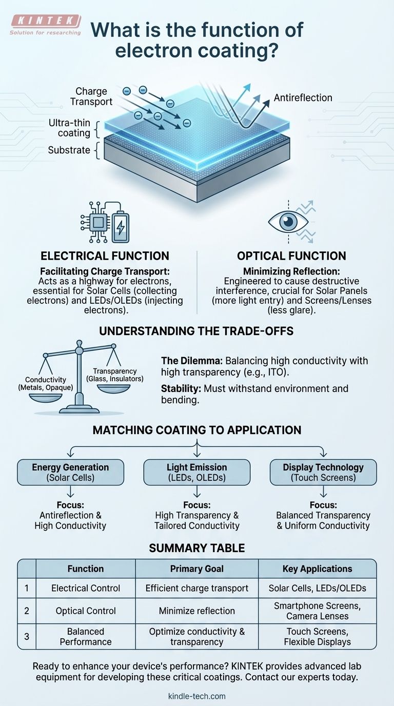
At its core, an electron coating is a specialized, ultra-thin film applied to a material to precisely control its electrical and optical properties. Rather than just a protective layer, its primary functions are to manage the flow of electrons (charge transport) and to manipulate how light interacts with a device's surface (antireflection), directly boosting performance and efficiency.
The term "electron coating" doesn't refer to a single material, but a class of functional layers. Their purpose isn't just protection; it's to actively enhance a device's core operation by guiding electrons and photons exactly where they are needed.
The Two Pillars of Function: Electrical and Optical Control
The value of these coatings comes from their ability to solve two fundamental problems in modern electronics: getting electricity to flow where it's needed and ensuring light isn't wasted. These are not secondary features; they are critical to the device's function.
Electrical Function: Facilitating Charge Transport
Charge transport is the movement of electrical charge—specifically electrons or the "holes" they leave behind—through a material. An effective coating acts as a dedicated highway for these charges.
Without an efficient path, electrons can get lost or trapped, reducing the device's performance. The coating provides a highly conductive and often transparent layer to collect or inject electrons.
This is essential in devices like solar cells, where the coating's job is to collect electrons generated by sunlight and channel them out to the external circuit. In LEDs and OLEDs, its role is reversed: to efficiently inject electrons into the light-emitting layer.
Optical Function: Minimizing Reflection
Every time light passes from one material to another (like from air to glass), a portion of that light reflects off the surface. This reflected light is wasted energy and can cause unwanted glare.
Antireflection coatings are engineered with a specific thickness and refractive index to cause reflected light waves to cancel each other out through destructive interference.
In a solar panel, this means more light enters the active material, generating more electricity. For a smartphone screen or camera lens, it means less glare and a clearer, brighter image for the user.
Understanding the Trade-offs
Choosing the right coating is an exercise in managing competing properties. No single material is perfect for every application, and engineers must balance critical performance metrics.
The Conductivity vs. Transparency Dilemma
The most common trade-off is between electrical conductivity and optical transparency. Materials that conduct electricity well (like metals) tend to be opaque, while materials that are highly transparent (like glass) are typically insulators.
This creates a major challenge for applications like touch screens and solar cells, which require a surface that is both highly transparent and uniformly conductive.
Materials like Indium Tin Oxide (ITO) are the industry standard because they offer the best-known compromise. However, ITO is expensive and brittle, driving research into alternative materials like silver nanowires, graphene, and conductive polymers.
Environmental and Mechanical Stability
A coating is useless if it degrades quickly. It must be robust enough to withstand the operating environment, including exposure to oxygen, humidity, and temperature changes.
Furthermore, for applications like flexible displays or wearable sensors, the coating must also be mechanically durable. It needs to bend without cracking or losing its conductive properties, a significant challenge for traditionally brittle materials like ITO.
Matching the Coating to the Application
The ideal coating is entirely dependent on the primary goal of your device. To make an informed decision, you must first define your priority.
- If your primary focus is energy generation (e.g., solar cells): You need a coating that excels at both antireflection to capture maximum light and high conductivity to efficiently extract the generated electrons.
- If your primary focus is light emission (e.g., LEDs, OLEDs): You need a coating with the highest possible transparency to let light out and tailored conductivity to inject charges precisely into the emissive layer.
- If your primary focus is display technology (e.g., touch screens): Your priority is the optimal balance between high transparency for image clarity and uniform conductivity for accurate sensing across the entire surface.
Ultimately, selecting the right electron coating is about defining your device's primary goal and choosing the material that best serves that specific function.
Summary Table:
| Function | Primary Goal | Key Applications |
|---|---|---|
| Electrical Control | Facilitate efficient charge transport | Solar Cells, LEDs/OLEDs |
| Optical Control | Minimize reflection (antireflection) | Smartphone Screens, Camera Lenses |
| Balanced Performance | Optimize conductivity & transparency | Touch Screens, Flexible Displays |
Ready to enhance your device's performance with the right electron coating?
At KINTEK, we specialize in providing advanced lab equipment and consumables for developing and testing these critical coatings. Whether you're working on next-generation solar cells, flexible displays, or high-efficiency LEDs, our solutions help you achieve precise control over electrical and optical properties.
Contact our experts today to discuss how we can support your specific laboratory needs and help you select the ideal materials for your application.
Visual Guide
Related Products
- Electron Beam Evaporation Coating Oxygen-Free Copper Crucible and Evaporation Boat
- Electron Beam Evaporation Coating Gold Plating Tungsten Molybdenum Crucible for Evaporation
- Electrolytic Electrochemical Cell for Coating Evaluation
- Electrode Polishing Material for Electrochemical Experiments
- Conductive Carbon Cloth Carbon Paper Carbon Felt for Electrodes and Batteries
People Also Ask
- What is the temperature of e-beam evaporation? Mastering the Two-Zone Thermal Process for Precision Films
- What is e-beam evaporation used for? Precision Coating for Optics, Aerospace & Electronics
- What is the voltage of e-beam evaporation? Achieve Precise Thin-Film Deposition
- What is the container that holds the metal source material called in e-beam evaporation? Ensure Purity and Quality in Your Thin-Film Deposition
- What are the applications of e-beam evaporation? Achieve High-Purity Coatings for Optics & Electronics