
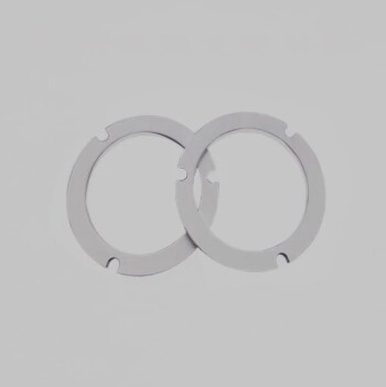
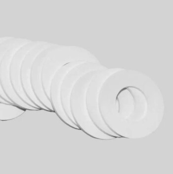
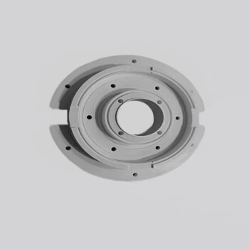
Thin Film Deposition Parts
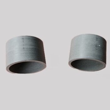
Electron Beam Evaporation Coating Conductive Boron Nitride Crucible BN Crucible
Item Number : KES03
Price varies based on specs and customizations
- Material
- Boron nitride
- Specification
- 35-64.5mm*17-35mm
Shipping:
Contact us to get shipping details Enjoy On-time Dispatch Guarantee.
Why Choose Us
Easy ordering process, quality products, and dedicated support for your business success.
Application
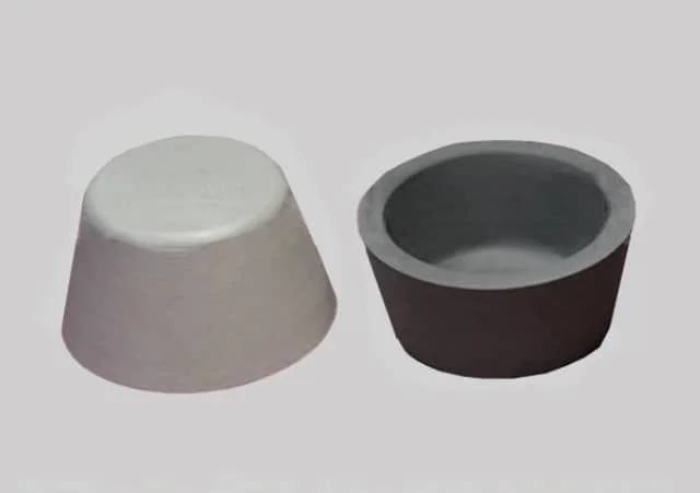
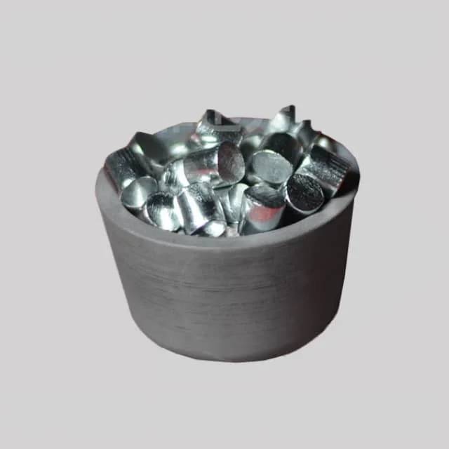
Conductive boron nitride crucibles are high-purity, smooth crucibles designed for electron beam evaporation coatings. It has excellent high temperature resistance and thermal cycle performance, and does not react with various metals and ceramic rare earths. The crucible remains intact even under rapid heating and cooling conditions. It has applications in alloy melting, rare earth and ceramic sintering, and electron beam evaporation coating. It is often used in thermal evaporation processes such as high-frequency induction heating, coating, electron beam evaporation coating, aluminum plating, and silicon plating.
The conductive boron nitride crucible has high purity, high finish, and excellent electron beam evaporation coating performance. They can increase evaporation rates, accelerate material switching, improve thermal stability and reduce power requirements, ultimately increasing productivity and cost efficiency.
Detail & Parts
Technical Specifications
| Outer diameter | 35mm | 40mm | 45mm | 50mm | 64.5mm |
| High | 17mm | 20mm | 22.5mm | 25mm | 35mm |
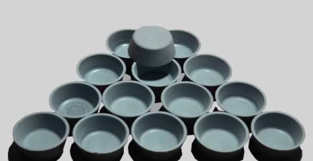
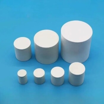
The crucibles we show are available in different sizes and custom sizes are available on request.
Advantage
- The film has good finish, high purity, less pollution and long service life.
- Excellent high temperature resistance, heat cycle resistance.
- Low thermal expansion, resists wetting by most molten metals.
- Heat resistance up to 2000℃, boron nitride does not react with aluminum and is not easy to volatilize.
- Increased evaporation rate; Increased evaporation rate reduces cycle time and increases overall yield.
- Fast material changeover; Conductive boron nitride crucibles facilitate fast material changeover, minimizing chamber downtime and increasing process efficiency.
- Enhanced Thermal Stability; These crucibles have increased thermal stability, reducing heat transfer from the crucible itself and ensuring consistent and controlled evaporation.
Trusted by Industry Leaders

FAQ
What Are Thermal Evaporation Sources?
What Are The Main Types Of Thermal Evaporation Sources?
How Do Thermal Evaporation Sources Work?
What Are The Common Materials Used For Evaporating Crucibles?
What Are The Advantages Of Using Thermal Evaporation Sources?
What Are The Advantages Of Using Evaporating Crucibles?
What Applications Are Thermal Evaporation Sources Used For?
How Should Evaporating Crucibles Be Handled And Maintained?
REQUEST A QUOTE
Our professional team will reply to you within one business day. Please feel free to contact us!
Related Products

Electron Beam Evaporation Coating Tungsten Crucible and Molybdenum Crucible for High Temperature Applications
Tungsten and molybdenum crucibles are commonly used in electron beam evaporation processes due to their excellent thermal and mechanical properties.
Boron Nitride (BN) Crucible for Phosphorous Powder Sintered
Phosphorus powder sintered boron nitride (BN) crucible has a smooth surface, dense, pollution-free and long service life.

Electron Beam Evaporation Coating Gold Plating Tungsten Molybdenum Crucible for Evaporation
These crucibles act as containers for the gold material evaporated by the electron evaporation beam while precisely directing the electron beam for precise deposition.

E Beam Crucibles Electron Gun Beam Crucible for Evaporation
In the context of electron gun beam evaporation, a crucible is a container or source holder used to contain and evaporate the material to be deposited onto a substrate.

Electron Beam Evaporation Coating Oxygen-Free Copper Crucible and Evaporation Boat
Electron Beam Evaporation Coating Oxygen-Free Copper Crucible enables precise co-deposition of various materials. Its controlled temperature and water-cooled design ensure pure and efficient thin film deposition.

High Purity Pure Graphite Crucible for Electron Beam Evaporation
A technology mainly used in the field of power electronics. It is a graphite film made of carbon source material by material deposition using electron beam technology.
Conductive Boron Nitride BN Ceramics Composite for Advanced Applications
Due to the characteristics of boron nitride itself, the dielectric constant and dielectric loss are very small, so it is an ideal electrical insulating material.
Boron Nitride (BN) Ceramic Rod for High Temperature Applications
Boron nitride (BN) rod is the strongest boron nitride crystal form like graphite, which has excellent electrical insulation, chemical stability and dielectric properties.

Boron Nitride (BN) Ceramic Plate
Boron nitride (BN) ceramic plates do not use aluminum water to wet, and can provide comprehensive protection for the surface of materials that directly contact molten aluminum, magnesium, zinc alloys and their slag.

Evaporation Crucible for Organic Matter
An evaporation crucible for organic matter, referred to as an evaporation crucible, is a container for evaporating organic solvents in a laboratory environment.
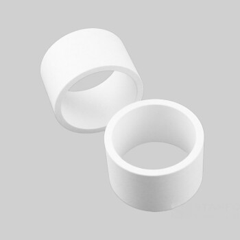
Boron Nitride (BN) Ceramic Tube
Boron nitride (BN) is known for its high thermal stability, excellent electrical insulating properties and lubricating properties.

High Purity Pure Graphite Crucible for Evaporation
Vessels for high temperature applications, where materials are kept at extremely high temperatures to evaporate, allowing thin films to be deposited on substrates.
Hexagonal Boron Nitride HBN Thermocouple Protection Tube
Hexagonal boron nitride ceramics is an emerging industrial material. Because of its similar structure to graphite and many similarities in performance, it is also called "white graphite".
Hexagonal Boron Nitride HBN Ceramic Ring
Boron nitride ceramic (BN) rings are commonly used in high temperature applications such as furnace fixtures, heat exchangers and semiconductor processing.

Laboratory CVD Boron Doped Diamond Materials
CVD boron-doped diamond: A versatile material enabling tailored electrical conductivity, optical transparency, and exceptional thermal properties for applications in electronics, optics, sensing, and quantum technologies.
Hexagonal Boron Nitride HBN Spacer Cam Profile and Various Spacer Types
Hexagonal boron nitride (HBN) gaskets are made from hot-pressed boron nitride blanks. Mechanical properties similar to graphite, but with excellent electrical resistance.
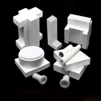
Custom Boron Nitride (BN) Ceramic Parts
Boron nitride (BN) ceramics can have different shapes, so they can be manufactured to generate high temperature, high pressure, insulation and heat dissipation to avoid neutron radiation.
Advanced Engineering Fine Ceramics Boron Nitride (BN) Ceramic Parts
Boron nitride ((BN) is a compound with high melting point, high hardness, high thermal conductivity and high electrical resistivity. Its crystal structure is similar to graphene and harder than diamond.

Ceramic Evaporation Boat Set Alumina Crucible for Laboratory Use
It can be used for vapor deposition of various metals and alloys. Most metals can be evaporated completely without loss. Evaporation baskets are reusable.1

Evaporation Boat for Organic Matter
The evaporation boat for organic matter is an important tool for precise and uniform heating during the deposition of organic materials.
Related Articles

Electron Beam Evaporation Coating Technology and Material Selection
An in-depth look at the principles and applications of electron beam evaporation coating technology, including material selection and various fields of application.
Guidelines for the Use of Boron Nitride Crucibles
Instructions on the proper use, precautions, and compatibility of boron nitride crucibles.
Electron Beam Evaporation: Advanced Thin Film Creation
Explores the technology and applications of electron beam evaporation in thin film production.
Electron Beam Evaporation Coating: Advantages, Disadvantages, and Applications
An in-depth look at the pros and cons of electron beam evaporation coating and its various applications in industries.
Electron Beam Evaporation Coating: Principles, Characteristics, and Applications
An in-depth analysis of electron beam evaporation coating technology, its advantages, disadvantages, and applications in thin film manufacturing.
Electron Beam Evaporation Technology in Vacuum Coating
An in-depth look at electron beam evaporation, its types, advantages, and disadvantages in vacuum coating processes.
The Role and Types of Crucibles in Scientific Experiments
Explores the significance and various types of crucibles in scientific experiments, focusing on their materials and applications.
Hexagonal Boron Nitride: Enhancing Performance in Composite Ceramic Materials
Explores the role of h-BN in various composite ceramics, highlighting its properties and applications.
Types of Evaporation Sources for Evaporative Coating
Explore different evaporation sources used in thin film deposition, including filaments, crucibles, and evaporation boats.
Alumina Crucibles in Precision Casting
Explores the use of alumina crucibles in precision casting, focusing on their properties and advantages in high-temperature alloy melting.
Preparation and Performance of Alumina Crucibles for Vacuum Induction Melting Furnace
This article discusses the preparation process and performance benefits of alumina crucibles for vacuum induction melting furnaces, emphasizing thermal stability and long service life.
Comprehensive Guide to Alumina Crucibles in Powder Metallurgy
An in-depth look at the properties, applications, and usage of alumina crucibles in powder metallurgy processes.