
Principle of Electron Beam Evaporation Coating Technology
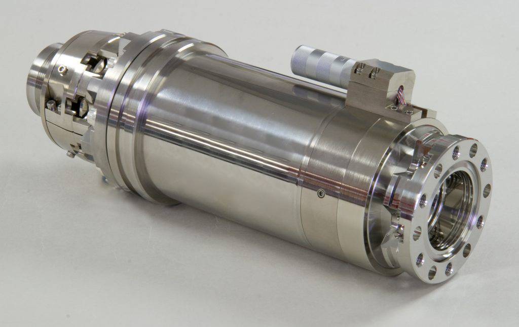
Types of Electron Beam Evaporation Sources
Electron beam evaporation sources are pivotal in the deposition of thin films, each type designed with specific structural and operational characteristics to cater to diverse material requirements. The ring gun and straight gun are foundational designs, with the former utilizing a circular profile for electron beam focus and the latter employing a linear trajectory. The E-type gun introduces an additional magnetic field to enhance beam concentration, while the hollow cathode gun leverages a unique cathode configuration to achieve high-density electron emission.
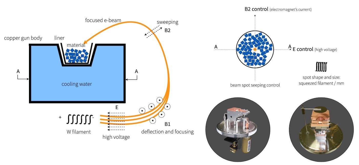
Each source type employs a coiled tungsten filament for thermionic emission, wherein electrons are released and subsequently accelerated through a magnetic field to bombard the target material. This bombardment generates sufficient heat to vaporize materials with exceptionally high melting points, making electron beam evaporation a versatile method for depositing both metallic and dielectric films.
The operational efficiency of these sources is further augmented by cooling water circulator systems, which prevent the co-deposition of the source material, typically copper. This cooling mechanism ensures that only the target material is vaporized, maintaining the purity and integrity of the deposited film. The chamber pressure is meticulously controlled to minimize background gas interference, thereby optimizing the deposition process for various applications, including lift-off, ohmic contacts, insulation, and optical coatings.
Process Steps in Electron Beam Evaporation
The electron beam evaporation process is a meticulously orchestrated sequence involving several critical steps: electron beam generation, acceleration, focusing, target bombardment, film deposition, and precise control parameters to ensure the desired film properties.
-
Electron Beam Generation and Acceleration: The process begins with the generation of an electron beam from a filament, typically made of tungsten, heated to temperatures exceeding 2,000 degrees Celsius. This extreme heat liberates electrons from the filament, imparting them with significant kinetic energy. These electrons are then accelerated through an electric field, typically ranging from 5 to 10 kV/cm, and focused into a coherent beam using magnets or electron lenses.
-
Target Bombardment: The focused electron beam is directed towards a e beam crucible containing the source material. The crucible, often made of materials like copper or tungsten crucible for lower temperature materials, or technical ceramics for higher temperature applications, is designed to withstand the intense heat without contaminating the source material. The electron beam's energy raises the temperature of the source material to its evaporation point, causing it to vaporize.
-
Film Deposition: The evaporated particles rise to the top of the vacuum chamber and condense on the substrate, forming a thin film. The deposition rate and film thickness are meticulously monitored in real-time using a quartz microplate. Once the desired film thickness is achieved, the electron beam is shut off, and the system initiates a cool-down and venting sequence to relieve the vacuum pressure.
-
Multi-Source Evaporation: Advanced systems often feature multiple crucibles, enabling the deposition of multiple layers of different materials without venting the chamber between layers. The electron beam source power can be adjusted to accommodate various coating materials, each requiring different heat intensities for evaporation.
This multi-step process ensures high thermal efficiency and purity, making electron beam evaporation a preferred method for applications demanding precise control over film properties.
Advantages of Electron Beam Evaporation
Electron beam evaporation stands out due to its high energy density, which allows it to achieve higher maximum evaporation temperatures compared to traditional thermal evaporation methods. This capability is particularly advantageous for vaporizing metals with high melting points, such as tungsten and molybdenum, ensuring that a wide range of materials can be effectively processed.
One of the key benefits of electron beam evaporation is its direct heating mechanism. By focusing the electron beam directly on the target material, the process avoids the need for a container, thereby eliminating the risk of contamination from crucible materials. This direct heating method also enhances thermal efficiency, as the energy is concentrated solely on the material to be evaporated, minimizing energy losses.
The process boasts rapid vapor deposition rates, ranging from 0.1 μm/min to 100 μm/min, which significantly speeds up the coating application. This rapid deposition results in high-density coatings with excellent adhesion, making the technique ideal for applications requiring robust and durable coatings. The high purity of the coatings is another notable advantage, as the focused electron beam minimizes the risk of contamination from surrounding materials.
Moreover, electron beam evaporation supports multi-layer deposition using various source materials without the need for venting between layers. This capability is particularly useful in creating complex coatings with tailored properties. The technology is also versatile, compatible with a broad spectrum of materials, including high-temperature metals and metal oxides, further expanding its application potential.
| Advantage | Description |
|---|---|
| High Energy Density | Enables higher evaporation temperatures, suitable for high-melting metals. |
| Direct Heating | Avoids container material evaporation, enhancing thermal efficiency and purity. |
| Rapid Deposition Rates | Fast coating application, ranging from 0.1 μm/min to 100 μm/min. |
| High-Density Coatings | Produces robust, durable coatings with excellent adhesion. |
| High Purity | Minimizes contamination risk, ensuring high-quality coatings. |
| Multi-Layer Deposition | Allows for complex coatings without the need for venting. |
| Material Versatility | Compatible with a wide range of materials, including high-temp metals and metal oxides. |
Selection of E-beam Coating Materials
Material Considerations
When selecting materials for electron beam evaporation coating, the choice is influenced by both the intended application and the specific process conditions. The primary goal is to ensure that the material can withstand the high-energy environment of the evaporation process while meeting the functional requirements of the final product.
Common materials used in this process can be broadly categorized into metals and non-metallic compounds. Metals such as gold, silver, and copper are frequently chosen due to their excellent electrical and thermal conductivity, making them ideal for applications in electronics and optics. These metals also have high melting points, which allows them to be vaporized efficiently without degrading.
On the other hand, non-metallic compounds like silicon dioxide (SiO₂) and silicon nitride (Si₃N₄) are valued for their dielectric properties and thermal stability. Silicon dioxide, for instance, is widely used in optical coatings due to its transparency and ability to modify the refractive index of the coating. Silicon nitride, with its high hardness and chemical inertness, is often employed in protective coatings for cutting tools and in microelectronic devices.
| Material Type | Examples | Primary Applications |
|---|---|---|
| Metals | Gold, Silver, Copper | Electronics, Optics, Conductive Coatings |
| Non-Metallic Compounds | Silicon Dioxide, Silicon Nitride | Optical Coatings, Protective Coatings, Microelectronics |
The selection process involves a careful balance between the material's physical and chemical properties and the demands of the application. For instance, in the aerospace industry, materials must endure extreme temperatures and pressures, while in the biomedical field, biocompatibility and non-toxicity are critical.
In summary, the choice of material in electron beam evaporation coating is a multifaceted decision that hinges on the interplay between application requirements, process conditions, and the intrinsic properties of the material. Each material brings its own set of advantages and challenges, making material selection a crucial step in the coating process.
Applications of E-beam Coating
E-beam technology finds extensive applications across a spectrum of industries, each leveraging its unique capabilities. In the realm of optics, E-beam coating is employed to create ultra-thin, high-quality layers that enhance the performance of lenses and mirrors, ensuring superior light transmission and reflection. This technology is also pivotal in the electronics sector, where it is used to deposit precise, conductive layers on semiconductor devices, contributing to enhanced functionality and reliability.
For magnetic materials, E-beam coating plays a crucial role in improving the magnetic properties of various components, such as hard drives and magnetic storage devices, by ensuring uniform and high-quality coatings. In the decorative coatings industry, E-beam technology is utilized to produce lustrous, durable finishes on products ranging from consumer goods to architectural elements, offering both aesthetic appeal and protection.
The cutting tool coatings sector benefits from E-beam technology by enabling the deposition of hard, wear-resistant layers that extend the lifespan of cutting tools and improve their performance in machining operations. In the energy sector, E-beam coating is applied to create efficient solar cells and other energy-related components, enhancing their performance and durability.
In the biomedical field, E-beam coating is used to develop biocompatible materials for medical devices, ensuring they are safe for use in the human body. The aerospace, defense, and nuclear industries also rely on E-beam technology for its ability to produce robust, high-performance coatings that can withstand extreme conditions, thereby enhancing the reliability and safety of critical components.
Each of these applications underscores the versatility and precision of E-beam coating, making it an indispensable technology across multiple industrial domains.
Related Products
- Electron Beam Evaporation Coating Tungsten Crucible and Molybdenum Crucible for High Temperature Applications
- Electron Beam Evaporation Coating Conductive Boron Nitride Crucible BN Crucible
- Electron Beam Evaporation Coating Oxygen-Free Copper Crucible and Evaporation Boat
- Electron Beam Evaporation Coating Gold Plating Tungsten Molybdenum Crucible for Evaporation
- High Purity Pure Graphite Crucible for Electron Beam Evaporation


