
Introduction to Electron Beam Evaporation
Process Overview
Electron Beam Evaporation is a sophisticated physical vapor deposition (PVD) technique, primarily utilized to create thin films on various substrates. This method operates within a high-vacuum environment, where an electron beam is directed towards a target material. The high-energy electron beam serves as the primary heating source, elevating the temperature of the material to the point of evaporation. As the material evaporates, it condenses onto a nearby substrate, forming a thin, uniform film.
The process is meticulously controlled to ensure precise film thickness and uniformity. The high-vacuum conditions are crucial as they minimize contamination and facilitate the deposition of high-purity films. This technique is particularly advantageous for materials with high melting points, as the direct heating by the electron beam allows for efficient vaporization without the need for a crucible, thereby avoiding any contamination from the container material.
In summary, Electron Beam Evaporation is a cornerstone in the production of thin films, offering high precision and purity, which are essential for a wide array of applications ranging from optical coatings to industrial uses.
Applications
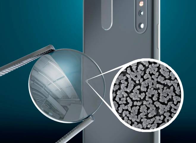
Electron beam evaporation finds extensive use across various sectors, particularly in the production of specialized coatings and films. One of its primary applications is in the creation of anti-reflective (AR) and anti-fingerprint (AF) coatings, which are essential for enhancing the optical properties of lenses and displays. These coatings reduce glare and improve visibility, making them indispensable in consumer electronics and optical instruments.
In addition to AR/AF coatings, this technology is also pivotal in the development of hard coatings. These coatings, known for their superior durability and resistance to wear, are commonly applied to cutting tools, surgical instruments, and other high-stress applications. The ability to create these robust films has significantly contributed to the longevity and performance of various industrial tools and equipment.
Decorative coatings are another noteworthy application. Electron beam evaporation enables the production of aesthetically pleasing and durable surface finishes, often used in the automotive and architectural industries. These coatings can mimic the appearance of precious metals or create unique color effects, adding both value and visual appeal to products.
The technology is also integral to the fabrication of indium tin oxide (ITO) films, which are crucial for transparent conductive coatings in touchscreens, solar cells, and flat-panel displays. ITO films produced via electron beam evaporation offer high conductivity and transparency, making them ideal for modern electronic devices.
Furthermore, electron beam evaporation is employed in the manufacturing of band pass filters and high-reflectivity (HR) films. Band pass filters are used in optical communication systems to selectively transmit specific wavelengths of light, while HR films are essential in laser technology and other high-precision optical applications.
Beyond these, the technology has significant industrial applications, particularly in the aerospace and tooling industries. In aerospace, it is used to create lightweight and durable components, while in tooling, it enhances the performance and lifespan of cutting and forming tools. This versatility underscores the broad impact of electron beam evaporation across multiple sectors.
Technological Principles
Types of Electron Guns
Electron guns are pivotal components in the electron beam evaporation process, each designed to address specific needs and limitations. The ring gun is particularly effective for materials that require uniform heating, such as those used in optical coatings. Its design allows for precise control over the beam's distribution, ensuring consistent film thickness.
The straight gun, on the other hand, is ideal for applications requiring high-energy beams, such as in the deposition of hard coatings. Its simplicity in design and operation makes it a reliable choice for industrial settings where robustness and ease of maintenance are crucial.
The e-type gun offers a balance between efficiency and versatility, making it suitable for a wide range of materials and applications. Its ability to generate a focused beam with high current density is advantageous in creating intricate patterns and high-quality films.
Lastly, the hollow cathode electron gun is notable for its efficiency in handling reactive materials, such as those used in the production of ITO films. Its unique structure allows for better control over the evaporation process, minimizing contamination and ensuring the purity of the deposited film.
Each type of electron gun has its own set of applications and limitations, contributing to the diversity and adaptability of electron beam evaporation technology.
Advantages
Electron beam evaporation boasts several key advantages that make it a preferred method for thin film creation. One of the most significant benefits is its high beam density. This high beam density ensures that the material being evaporated is subjected to uniform heating, which is crucial for maintaining the consistency and quality of the resulting thin film.
Another notable advantage is the avoidance of container material evaporation. Traditional methods often suffer from contamination due to the evaporation of the container material, which can degrade the quality of the thin film. Electron beam evaporation circumvents this issue by directly heating the target material without the need for a container, thereby ensuring a purer final product.
The process also features direct heat addition to the surface of the vaporized material. This direct application of heat allows for precise control over the temperature and energy distribution, leading to more accurate and predictable film formation. This level of control is essential for achieving the desired properties in the thin film, such as optical transparency, electrical conductivity, or mechanical hardness.
Lastly, electron beam evaporation offers high thermal efficiency. The method efficiently converts electrical energy into thermal energy, minimizing energy losses and reducing operational costs. This efficiency is particularly beneficial in industrial settings where large-scale production is required, as it can significantly lower the overall cost of thin film manufacturing.
| Advantage | Description |
|---|---|
| High Beam Density | Ensures uniform heating and consistent film quality. |
| Avoidance of Container Material Evaporation | Prevents contamination and ensures a purer final product. |
| Direct Heat Addition | Allows for precise temperature control and predictable film formation. |
| High Thermal Efficiency | Minimizes energy losses and reduces operational costs. |
These advantages collectively enhance the effectiveness and reliability of electron beam evaporation, making it a cornerstone technology in the production of advanced thin films.
Future Trends and Developments
Equipment Upgrades
The evolution in electron beam evaporation technology is marked by a significant shift from traditional single evaporation systems to advanced multi-functional, high-speed, and high-efficiency integrated systems. These modern systems are designed to optimize the deposition process, enhancing both productivity and the quality of the thin films produced.
One of the key advancements in these integrated systems is the ability to perform multiple functions within a single unit. This includes simultaneous evaporation of multiple materials, precise control over the deposition rate, and the incorporation of advanced monitoring and feedback mechanisms. Such capabilities not only streamline the production process but also ensure greater consistency and reliability in the final product.
Moreover, the integration of high-speed components allows for faster evaporation cycles, thereby increasing throughput without compromising on the quality of the deposited films. High-efficiency features, such as improved energy utilization and reduced material wastage, further contribute to the sustainability and economic viability of these systems.
In summary, the transition to multi-functional, high-speed, high-efficiency integrated systems represents a major leap forward in the field of electron beam evaporation, paving the way for more sophisticated and efficient thin film production technologies.
Material Innovations
The future of electron beam evaporation lies in the innovative incorporation of polymer materials and advanced deposition techniques. These innovations are poised to significantly enhance the properties and applications of thin films. By integrating polymers, which offer unique mechanical, thermal, and electrical properties, the versatility of thin films can be expanded. This integration allows for the creation of films with tailored characteristics, suitable for a broader range of applications, from flexible electronics to biomedical devices.
New deposition techniques, such as atomic layer deposition (ALD) and pulsed laser deposition (PLD), are also being explored to complement traditional methods. These techniques provide greater control over film thickness and uniformity, essential for applications requiring precise film properties. For instance, ALD's ability to deposit materials layer-by-layer with atomic precision makes it ideal for creating high-performance coatings for optical and electronic devices.
| Material Type | Deposition Technique | Application |
|---|---|---|
| Polymers | Electron Beam Evaporation | Flexible Electronics |
| Metals | Atomic Layer Deposition | Optical Coatings |
| Composites | Pulsed Laser Deposition | Biomedical Devices |
The synergy between these materials and techniques not only improves the functional properties of thin films but also opens up new avenues for research and development. This dynamic interplay is expected to drive the next generation of thin film technologies, addressing current challenges and paving the way for innovative solutions in various industries.
Challenges and Solutions
Developing more efficient materials and technologies through electron beam evaporation is not without its challenges. One of the primary issues is film composition control. Ensuring that the film's chemical composition remains consistent throughout the deposition process is crucial for maintaining the desired properties of the thin film. This requires precise control over the evaporation rate and the distribution of the evaporated material.
Another significant challenge is the formation of microstructures within the film. The microstructure of the film can significantly impact its mechanical, electrical, and optical properties. Controlling the microstructure involves managing factors such as substrate temperature, deposition rate, and the presence of any reactive gases in the vacuum chamber.
Cost is another critical factor. The development of advanced materials and technologies often comes with high initial costs, which can be a barrier to widespread adoption. Solutions to this challenge include optimizing the process to reduce material waste, improving the efficiency of the deposition equipment, and exploring cost-effective alternatives for both the materials and the deposition techniques.
By addressing these challenges, researchers and engineers can push the boundaries of what is possible with electron beam evaporation, leading to the creation of more efficient and versatile thin films for a wide range of applications.
Related Products
- Electron Beam Evaporation Coating Tungsten Crucible and Molybdenum Crucible for High Temperature Applications
- Electron Beam Evaporation Coating Oxygen-Free Copper Crucible and Evaporation Boat
- Electron Beam Evaporation Coating Conductive Boron Nitride Crucible BN Crucible
- Electron Beam Evaporation Coating Gold Plating Tungsten Molybdenum Crucible for Evaporation
- E Beam Crucibles Electron Gun Beam Crucible for Evaporation
Related Articles
- The Role and Types of Crucibles in Scientific Experiments
- Alumina Crucibles in Precision Casting
- Electron Beam Evaporation Coating: Advantages, Disadvantages, and Applications
- Electron Beam Evaporation Coating: Principles, Characteristics, and Applications
- Comprehensive Guide to Alumina Crucibles in Powder Metallurgy


