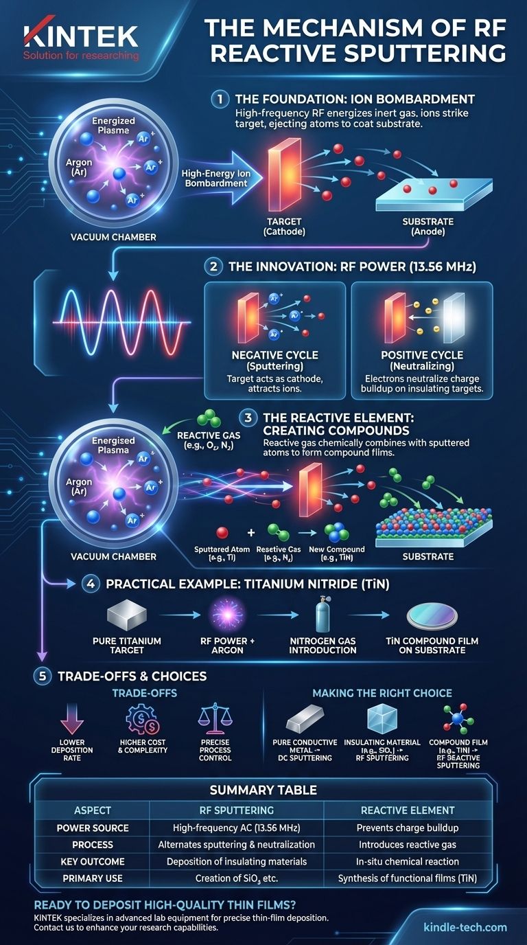
RF reactive sputtering is a thin-film deposition technique that combines two key principles. It uses a high-frequency alternating current (RF) to dislodge atoms from a target material, a method uniquely suited for non-conductive materials. Simultaneously, it introduces a reactive gas, like oxygen or nitrogen, into the vacuum chamber to chemically combine with the sputtered atoms, forming a new compound film on the substrate.
At its core, RF reactive sputtering is the definitive solution for creating high-quality, complex compound films (like oxides and nitrides), especially from targets that are electrical insulators. The RF power prevents charge buildup on the target, while the reactive gas engineers the final chemical composition of the deposited film.
The Foundation: How Sputtering Works
The Core Principle: Ion Bombardment
Sputtering begins in a high-vacuum chamber filled with an inert gas, typically argon. A strong electric field energizes this gas, creating a glowing plasma of positively charged argon ions and free electrons.
The material to be deposited, known as the target, is set up as a cathode (a negative electrode).
The positive argon ions in the plasma are forcefully accelerated toward the negatively charged target, striking its surface with significant kinetic energy.
From Target to Substrate
This high-energy ion bombardment physically ejects, or "sputters," individual atoms from the target material.
These sputtered atoms travel through the vacuum chamber and condense onto a substrate (such as a silicon wafer), gradually building up a thin film of the target material.
The Innovation: Adding Radio Frequency (RF)
The Problem with Insulating Targets
In basic DC sputtering, the target must be electrically conductive. If you use an insulating (dielectric) target, positive argon ions accumulate on its surface.
This buildup of positive charge, known as charging, eventually repels incoming argon ions, effectively stopping the sputtering process.
The RF Solution: Alternating Polarity
RF sputtering solves this problem by replacing the DC power supply with a high-frequency AC power source, typically fixed at 13.56 MHz.
This rapidly alternates the target's electrical potential between negative and positive, preventing a static charge from ever accumulating.
The Negative Cycle: Sputtering the Target
During the brief negative portion of the AC cycle, the target behaves as it would in DC sputtering. It attracts positive argon ions, which bombard the surface and eject target atoms.
The Positive Cycle: Neutralizing Charge
During the subsequent positive cycle, the target attracts a shower of free electrons from the plasma. This influx of negative charge completely neutralizes the positive ion buildup from the previous cycle.
This rapid, continuous cycle of sputtering and neutralizing allows for the uninterrupted deposition of insulating materials.
The "Reactive" Element: Creating New Compounds
Moving Beyond Inert Gas
In standard sputtering (both DC and RF), the goal is to deposit a film that is identical to the target material.
Reactive sputtering introduces a second gas into the chamber: a reactive gas like oxygen or nitrogen.
The Chemical Reaction in the Chamber
As atoms are sputtered from the target, they travel toward the substrate through an environment containing both argon and the reactive gas.
During this transit, the sputtered atoms chemically react with the gas to form a new compound. This reaction can occur in the plasma or directly on the substrate surface.
A Practical Example: Creating Titanium Nitride
To create a hard coating of titanium nitride (TiN), you would use a pure titanium target.
By introducing nitrogen gas along with the standard argon, the sputtered titanium atoms react with the nitrogen to form a TiN compound film on the substrate.
Understanding the Trade-offs
Deposition Rate
RF sputtering generally has a lower deposition rate compared to DC sputtering. The process is less efficient because sputtering only occurs during the negative half of the power cycle.
Cost and Complexity
The RF power supplies and matching networks required are significantly more complex and expensive than DC power supplies. This often makes RF sputtering better suited for smaller substrates.
Process Control
In reactive sputtering, the process becomes a delicate balancing act. The ratio of inert gas to reactive gas must be precisely controlled to achieve the desired film stoichiometry and prevent poisoning the target surface.
Making the Right Choice for Your Goal
Your choice of sputtering technique must align directly with the material you intend to deposit and the final film composition you require.
- If your primary focus is depositing a pure, conductive metal: DC sputtering is typically the more efficient and cost-effective choice.
- If your primary focus is depositing an insulating material (like SiO₂): Standard RF sputtering is necessary to prevent charge buildup on the dielectric target.
- If your primary focus is creating a specific compound film (like an oxide or nitride): RF reactive sputtering is the essential method, allowing you to synthesize the compound in-situ during deposition.
Understanding this mechanism empowers you to select and control a process that transforms simple targets into complex, functional thin films.
Summary Table:
| Aspect | RF Sputtering | Reactive Element | Key Outcome |
|---|---|---|---|
| Power Source | High-frequency AC (13.56 MHz) | - | Prevents charge buildup on insulating targets |
| Process | Alternates between sputtering (negative cycle) and charge neutralization (positive cycle) | Introduces reactive gas (e.g., O₂, N₂) | Enables in-situ chemical reaction to form compounds |
| Primary Use | Deposition of insulating materials (e.g., SiO₂) | Creation of compound films (e.g., TiN, Al₂O₃) | Synthesis of high-quality functional thin films |
Ready to deposit high-quality insulating or compound thin films?
At KINTEK, we specialize in providing advanced lab equipment and consumables for precise thin-film deposition. Whether you're working with insulating targets or need to synthesize complex oxides and nitrides, our expertise in sputtering technologies can help you achieve superior results with controlled stoichiometry and film quality.
Let our team assist you in selecting the right equipment for your specific laboratory needs.
Contact us today to discuss your project and discover how KINTEK can enhance your research and development capabilities.
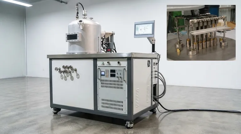
Visual Guide
Related Products
- RF PECVD System Radio Frequency Plasma-Enhanced Chemical Vapor Deposition RF PECVD
- Spark Plasma Sintering Furnace SPS Furnace
People Also Ask
- What is plasma CVD? Unlock Low-Temperature Thin Film Deposition for Sensitive Materials
- What is an example of PECVD? RF-PECVD for High-Quality Thin Film Deposition
- What is plasma chemical vapor deposition? A Low-Temperature Thin Film Coating Solution
- Why is a Matching Network Indispensable in RF-PECVD for Siloxane Films? Ensure Stable Plasma and Uniform Deposition
- What is plasma enhanced chemical vapour deposition PECVD used for? Enable Low-Temp Thin Films for Electronics & Solar

