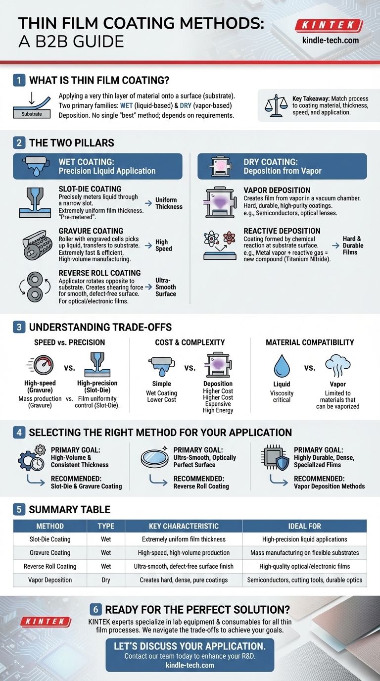
The method of thin film coating is not a single technique but a category of processes used to apply a very thin layer of material onto a surface, or "substrate." These methods are broadly divided into two families: liquid-based "wet coating" and vapor-based "dry coating" or deposition. The most common commercial wet coating methods include slot-die, gravure, and reverse roll coating, while vapor deposition involves processes that build the film atom-by-atom.
The critical takeaway is that there is no single "best" method. The choice depends entirely on matching the process to the specific requirements of the coating material, the desired film thickness, production speed, and final product application.
The Two Pillars of Thin Film Coating
To understand thin film application, it's essential to differentiate between the two primary approaches: applying a liquid that later dries, or depositing a solid material from a vapor.
Wet Coating Methods: Precision Liquid Application
Wet coating involves applying a liquid solution onto a substrate and then drying it to leave behind a solid film. This is common for polymers, adhesives, and optical layers on flexible materials like plastic films or paper.
Slot-Die Coating
A slot-die coater precisely meters and applies liquid through a narrow, machined slot directly onto the moving substrate.
This method is highly valued for its ability to produce extremely uniform film thicknesses across the entire width of the substrate. It is a "pre-metered" technique, meaning the amount of coating is determined before it's applied.
Gravure Coating
Gravure coating uses a roller that is engraved with a pattern of very small cells. This roller picks up the coating liquid, a doctor blade scrapes off the excess, and the roller then transfers the liquid from its cells onto the substrate.
It is an extremely fast and efficient method, making it ideal for high-volume manufacturing. The volume of transferred liquid is controlled by the size and density of the cells on the roller.
Reverse Roll Coating
This technique uses a series of rollers to meter and apply a highly uniform layer of coating. Crucially, the applicator roller rotates in the opposite direction of the moving substrate.
This "reverse" action creates a shearing force that smooths the liquid, resulting in an exceptionally smooth, defect-free surface finish. It is often used for high-quality optical or electronic films where surface quality is paramount.
Dry Coating Methods: Deposition from Vapor
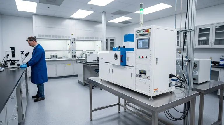
Dry coating, or deposition, involves creating a film from material in a vapor phase within a vacuum chamber. This is standard for creating hard, durable, or highly pure coatings like those on semiconductor wafers, cutting tools, and optical lenses.
Reactive Deposition
Reactive deposition is a process where the coating is formed by a chemical reaction at the substrate surface.
For example, a metal source material (like titanium) is vaporized in the presence of a reactive gas (like nitrogen). The metal and gas react to form a new compound (titanium nitride) directly on the product, creating a very hard and durable film. This is often a sub-category of physical or chemical vapor deposition.
Understanding the Trade-offs
Choosing a coating method involves balancing competing priorities. An expert decision requires understanding the inherent compromises of each technique.
Speed vs. Precision
High-speed methods like gravure coating are excellent for mass production but may offer less control over film uniformity compared to the slower, more precise slot-die method.
Cost and Complexity
Wet coating systems are generally less complex and have a lower capital cost than vapor deposition systems. Deposition requires expensive vacuum chambers, high-purity source materials, and significant energy input, but it can create films that are impossible to make with wet coating.
Material Compatibility
The properties of the coating liquid—especially its viscosity (thickness)—are critical. A low-viscosity liquid that works well for gravure coating might be unsuitable for a slot-die system. Similarly, deposition is limited to materials that can be vaporized or "sputtered."
Selecting the Right Method for Your Application
Your final choice is dictated by the end goal. A clear understanding of your primary objective will guide you to the correct process.
- If your primary focus is high-volume production with consistent thickness: Slot-die and gravure coating are often the most effective choices for liquid applications.
- If your primary focus is achieving an ultra-smooth, optically perfect surface: Reverse roll coating provides exceptional control over surface quality.
- If your primary focus is creating highly durable, dense, or specialized electronic films: Vapor deposition methods are the industry standard for performance and purity.
Understanding these fundamental differences empowers you to select a coating process that aligns perfectly with your technical and commercial goals.
Summary Table:
| Method | Type | Key Characteristic | Ideal For |
|---|---|---|---|
| Slot-Die Coating | Wet | Extremely uniform film thickness | High-precision liquid applications |
| Gravure Coating | Wet | High-speed, high-volume production | Mass manufacturing on flexible substrates |
| Reverse Roll Coating | Wet | Ultra-smooth, defect-free surface finish | High-quality optical/electronic films |
| Vapor Deposition | Dry | Creates hard, dense, pure coatings | Semiconductors, cutting tools, durable optics |
Ready to find the perfect thin film coating solution for your lab?
Choosing the right method is critical for the success of your project. The experts at KINTEK specialize in lab equipment and consumables for all thin film coating processes. We can help you navigate the trade-offs between speed, precision, and material compatibility to achieve your technical and commercial goals.
Let's discuss your application. Contact our team today to get personalized advice and discover how our solutions can enhance your research and development.
Visual Guide
Related Products
- Aluminized Ceramic Evaporation Boat for Thin Film Deposition
- Electron Beam Evaporation Coating Oxygen-Free Copper Crucible and Evaporation Boat
- Vacuum Hot Press Furnace Machine for Lamination and Heating
- Molybdenum Tungsten Tantalum Evaporation Boat for High Temperature Applications
- HFCVD Machine System Equipment for Drawing Die Nano-Diamond Coating
People Also Ask
- Why is an alumina boat selected for catalyst precursors? Ensure Sample Purity at 1000 °C
- Why are high-purity ceramic boats used for lignin activation? Ensure Purity & Thermal Stability
- What is the source of evaporation for thin film? Choosing Between Thermal and E-Beam Methods
- What are the applications of thin films deposition? Unlock New Possibilities for Your Materials
- What is the chemical method for thin film deposition? Build Films from the Molecular Level Up


