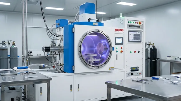
At its core, DC sputtering is a vacuum deposition technique that uses an ionized gas to physically eject atoms from a source material, known as a "target." These dislodged atoms then travel through the vacuum and deposit onto a surface, or "substrate," building up a thin film atom by atom. The entire process is driven by a high-voltage direct current (DC) electric field, which creates and directs the ionized gas.
The key to understanding DC sputtering is to think of it not as a chemical reaction, but as a physical momentum transfer. It is a subatomic "sandblasting" process where high-energy gas ions collide with a target, knocking loose the material you wish to deposit as a coating.

The Fundamental Mechanism: From Plasma to Film
The DC sputtering process is a sequence of well-defined physical events that occur within a vacuum chamber. Each step is critical for transforming a solid block of material into a high-precision thin film.
Step 1: Creating the Vacuum Environment
First, the target and substrate are placed inside a vacuum chamber, and most of the air is pumped out. This is essential to remove unwanted atoms and molecules that could contaminate the final film.
Once a vacuum is achieved, a small, controlled amount of an inert gas—most commonly Argon (Ar)—is introduced into the chamber.
Step 2: Applying the Electric Field
A high-voltage DC power supply is connected between the target and the chamber. The target is given a strong negative charge (making it the cathode), while the substrate holder and chamber walls act as the positive side (the anode).
This creates a powerful electric field throughout the low-pressure Argon gas.
Step 3: Igniting the Plasma
This electric field accelerates stray electrons naturally present in the gas. As these energetic electrons collide with neutral Argon atoms, they knock an electron off the Argon atom.
This creates a positively charged Argon ion (Ar+) and a new free electron. This process cascades rapidly, creating a self-sustaining cloud of ions and electrons known as a plasma, which is often visible as a characteristic glow.
Step 4: The Bombardment Process
The positively charged Argon ions (Ar+) are now strongly accelerated by the electric field directly toward the negatively charged target.
These ions strike the target surface with significant kinetic energy. The impact sets off a "collision cascade" within the target material, transferring momentum until atoms at the surface are physically ejected, or "sputtered," into the vacuum.
Step 5: Deposition onto the Substrate
The sputtered atoms from the target travel through the vacuum chamber. When they reach the substrate, they condense on its surface.
This process builds up, layer by layer, to form a dense and uniform thin film with precisely controlled properties like thickness and density.
Key Components of a DC Sputtering System
To understand the principle, it helps to know the role of each component.
The Target (The Source Material)
This is a solid piece of the material you want to deposit as a film (e.g., titanium, aluminum, gold). In DC sputtering, this material must be electrically conductive to maintain the negative charge.
The Substrate (The Destination)
This is the object you are coating. It can be anything from a silicon wafer for microelectronics to a piece of glass for an optical coating. It is placed on or near the anode.
The Sputtering Gas (The "Abrasive" Medium)
This is the inert gas, typically Argon, used to create the plasma. It is chosen because it is heavy enough to effectively sputter most materials but is chemically inert, meaning it won't react with the growing film.
The Power Supply (The Driving Force)
The DC power supply provides the energy that creates the electric field, ignites the plasma, and accelerates the ions—the three actions that drive the entire sputtering process.
Understanding the Trade-offs of DC Sputtering
While powerful, DC sputtering is not a universal solution. Its operating principle creates specific limitations that are crucial to understand.
The Conductivity Limitation
The single biggest constraint of DC sputtering is that it only works for conductive target materials. If you attempt to sputter an insulator (like a ceramic), the positive charge from the bombarding Argon ions will build up on the target's surface.
This "charge-up" effect quickly neutralizes the negative potential of the target, which shuts down the electric field and stops the sputtering process entirely. For insulating materials, a different technique like RF (Radio Frequency) sputtering is required.
Lower Deposition Rates
Compared to more advanced techniques like magnetron sputtering (which uses magnets to enhance the plasma), basic DC sputtering can be a relatively slow process. This can impact throughput in industrial applications.
Substrate Heating
The constant bombardment of particles and condensing atoms releases energy, which can significantly heat the substrate. This may be undesirable for coating heat-sensitive materials like plastics or certain biological samples.
Making the Right Choice for Your Application
Selecting a deposition method depends entirely on your material and the desired outcome of your film.
- If your primary focus is depositing a simple, conductive metal film: DC sputtering is a highly reliable, cost-effective, and well-understood method for creating high-purity metallic coatings.
- If your primary focus is depositing an insulating material (like an oxide or nitride): DC sputtering is unsuitable; you must use a technique like RF Sputtering, which overcomes the charge-up effect on the target.
- If your primary focus is achieving the highest possible deposition speed for a conductive target: You should consider magnetron sputtering, which is an enhancement of DC sputtering that uses magnetic fields to increase plasma density and sputtering efficiency.
Understanding this principle of physical momentum transfer is the key to controlling the growth of thin films at the atomic level.
Summary Table:
| Aspect | Description |
|---|---|
| Process Type | Physical Vapor Deposition (PVD) |
| Key Mechanism | Momentum transfer from ion bombardment |
| Target Material | Electrically Conductive (e.g., Metals) |
| Sputtering Gas | Inert Gas (Typically Argon) |
| Primary Limitation | Cannot sputter insulating materials |
Ready to achieve precise, high-purity conductive coatings for your lab? KINTEK specializes in providing reliable lab equipment and consumables for thin film deposition. Whether you are working with metals for microelectronics or optical coatings, our expertise ensures you get the right solution for your specific needs. Contact our experts today to discuss how we can support your laboratory's thin film research and production goals.
Visual Guide

Related Products
People Also Ask
- What is the recommended cleaning procedure for a carbon fiber brush after use? Extend Brush Life and Maintain Performance
- Why is it important to prevent mechanical damage to a carbon fiber brush? Ensure Peak Performance & Longevity
- What environmental conditions should be avoided when operating or storing a carbon fiber brush? Protect Your Investment from Damage
- What parameters require monitoring during an experiment involving a carbon fiber brush? Ensure Reliable Results
- What does the regular maintenance inspection of a carbon fiber brush entail? Ensure Peak Performance and Longevity
