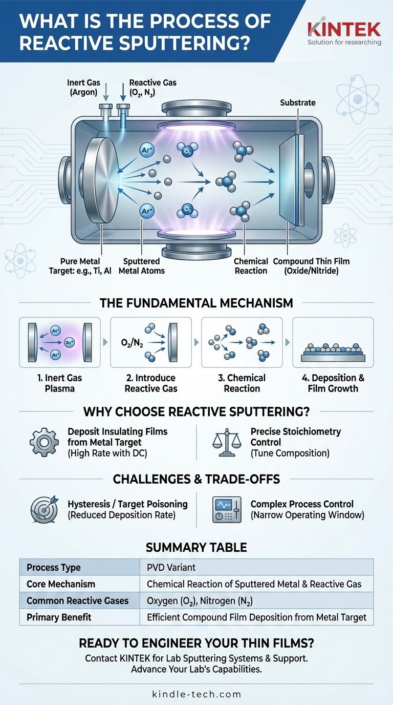
In essence, reactive sputtering is a thin-film deposition process that creates a compound material by introducing a reactive gas into a standard sputtering environment. Instead of simply depositing a pure metal from a target, this method uses a gas like oxygen or nitrogen to induce a chemical reaction, transforming the sputtered metal atoms into an oxide or nitride film on the substrate's surface.
The core principle of reactive sputtering is not about depositing what's on the target, but about creating a new material in the process. By precisely controlling the mixture of an inert sputtering gas and a reactive gas, you can form high-quality compound films from a simple metal target.
The Fundamental Mechanism: From Metal to Compound
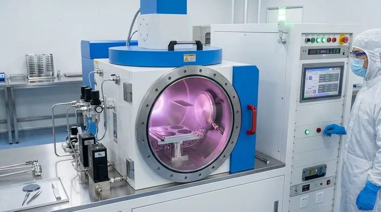
Reactive sputtering is a powerful variation of a standard Physical Vapor Deposition (PVD) technique. The process occurs within a vacuum chamber and involves several distinct steps to build the final film.
The Role of the Inert Gas (Argon)
First, the vacuum chamber is pumped down to a very low pressure. An inert gas, most commonly argon (Ar), is then introduced. Applying a high voltage creates a plasma, which is a state of matter containing energized, positively charged argon ions.
These argon ions are accelerated toward the target, which is a plate of pure source material (e.g., titanium, aluminum, silicon). The impact of these ions physically knocks atoms off the target in a process known as sputtering.
The Introduction of the Reactive Gas
This is the defining step of reactive sputtering. A second, reactive gas—typically oxygen (O2) or nitrogen (N2)—is carefully introduced into the chamber along with the argon.
The flow rate of this gas is a critical control parameter. It determines the nature and composition of the final film.
The Chemical Reaction and Deposition
As the sputtered metal atoms travel from the target to the substrate, they collide and chemically react with the molecules of the reactive gas. This reaction can occur in the space between the target and substrate or directly on the substrate surface itself.
For example, sputtered titanium atoms will react with nitrogen gas to form titanium nitride (TiN). The resulting compound molecules then condense on the substrate (such as a silicon wafer or tool steel), building up a thin film with completely different properties than the original metal target.
Why Choose Reactive Sputtering?
Engineers and scientists choose this method to solve specific challenges that other deposition techniques handle less effectively. Its benefits are primarily related to material flexibility and process efficiency.
Depositing Insulating Films from a Metal Target
Many valuable compound films, like aluminum oxide (Al₂O₃) or silicon nitride (Si₃N₄), are electrical insulators. Sputtering these "dielectric" materials directly from a ceramic target is possible, but it requires expensive Radio Frequency (RF) power supplies and often results in very low deposition rates.
Reactive sputtering provides a clever workaround. You can use a cheaper, more efficient Direct Current (DC) power supply to sputter a conductive metal target (like aluminum or silicon) while the reactive gas forms the desired insulating film.
Achieving Precise Stoichiometry
The process offers exceptional control over the chemical makeup, or stoichiometry, of the deposited film. By carefully adjusting the partial pressure of the reactive gas, you can create a wide spectrum of materials.
This allows for the creation of sub-stoichiometric films, fully stoichiometric films, or even complex graded layers where the composition changes with the film's thickness.
Understanding the Trade-offs and Challenges
While powerful, reactive sputtering is a complex process with critical trade-offs that require careful management for successful and repeatable results.
The "Hysteresis Effect" and Target Poisoning
The most significant challenge is a phenomenon known as hysteresis, or target poisoning. If the flow of reactive gas is too high, the reactive gas begins to form a compound layer on the surface of the sputtering target itself.
An oxidized or nitrided target surface sputters much more slowly than a pure metal one. This leads to a sudden and dramatic drop in the deposition rate. Managing the process to stay in the high-rate "metallic mode" without fully poisoning the target is a key operational skill.
Process Control Complexity
The optimal window for reactive sputtering is often very narrow. The process is highly sensitive to the balance between pumping speed, gas flow rates, and plasma power. Achieving a stable and repeatable deposition rate requires sophisticated feedback control systems that monitor the process in real-time.
Deposition Rate vs. Other Methods
While reactive sputtering from a metal target is generally faster than RF sputtering a ceramic target, it is inherently slower than sputtering the pure metal in a non-reactive process. The chemical reaction itself consumes energy and particles that would otherwise contribute to film growth.
Making the Right Choice for Your Goal
Selecting a deposition method depends entirely on the properties you need in your final film. Reactive sputtering is a specialized tool for creating compound materials.
- If your primary focus is depositing a dielectric film (like SiO₂ or Al₂O₃) at a high rate: Reactive sputtering a metal target (Si or Al) is often more efficient and cost-effective than RF sputtering a ceramic target directly.
- If you need to fine-tune the chemical composition of a film (e.g., titanium oxynitride): The precise gas flow control in reactive sputtering gives you direct command over the film's stoichiometry and properties.
- If your goal is to deposit a pure metal or a simple alloy: Standard non-reactive sputtering is the more straightforward and faster process.
By understanding its principles and controlling the reaction, you can leverage reactive sputtering to engineer a vast range of high-performance compound materials.
Summary Table:
| Key Aspect | Description |
|---|---|
| Process Type | Physical Vapor Deposition (PVD) variant |
| Core Mechanism | Chemical reaction between sputtered metal atoms and reactive gas |
| Common Reactive Gases | Oxygen (O₂), Nitrogen (N₂) |
| Common Targets | Pure metals (e.g., Titanium, Aluminum, Silicon) |
| Primary Benefit | Deposits insulating/compound films efficiently from a conductive metal target |
| Key Challenge | Managing target poisoning and the hysteresis effect for stable deposition |
Ready to Engineer Your Next-Generation Thin Films?
Reactive sputtering is a powerful technique for creating precise compound materials like oxides and nitrides. If you are developing coatings for optics, semiconductors, or wear-resistant tools, KINTEK's expertise in lab sputtering systems and consumables can help you achieve optimal results.
We provide the equipment and support to master complex processes like gas flow control and hysteresis management, ensuring high-quality, repeatable depositions for your R&D or production needs.
Contact KINTEK today to discuss how our reactive sputtering solutions can advance your laboratory's capabilities.
Visual Guide
Related Products
- Spark Plasma Sintering Furnace SPS Furnace
- Chemical Vapor Deposition CVD Equipment System Chamber Slide PECVD Tube Furnace with Liquid Gasifier PECVD Machine
- RF PECVD System Radio Frequency Plasma-Enhanced Chemical Vapor Deposition RF PECVD
- Customer Made Versatile CVD Tube Furnace Chemical Vapor Deposition Chamber System Equipment
- Vacuum Induction Melting Spinning System Arc Melting Furnace
People Also Ask
- Why are Spark Plasma Sintering (SPS) furnaces or hot presses utilized in the preparation of Li3PS4 solid electrolytes?
- What is the theory of spark plasma sintering? A Guide to Rapid, Low-Temperature Densification
- What is the mechanism of SPS process? A Deep Dive into Rapid, Low-Temperature Sintering
- What are the advantages of CAMI/SPS for W-Cu composite preparation? Reduce cycles from hours to seconds.
- What is SPS sintering method? A Guide to High-Speed, High-Performance Material Fabrication


