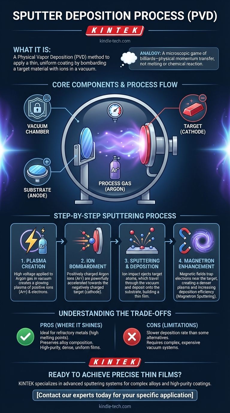
In essence, sputter deposition is a physical vapor deposition (PVD) method used to apply an extremely thin, uniform coating of one material onto another. The process involves bombarding a source material (the "target") with high-energy ions inside a vacuum. This collision physically ejects atoms from the target, which then travel through the vacuum and deposit onto the surface of a second object (the "substrate"), forming a film.
Sputtering is best understood as a microscopic game of billiards. It is not a chemical reaction or a melting process, but a physical momentum transfer. This distinction is the key to why it is so effective for depositing materials with very high melting points or complex compositions.
The Core Components of a Sputtering System
To understand the process, you must first understand its environment. A sputtering system is a carefully controlled setup designed for one purpose: moving atoms from a source to a destination with high purity and precision.
The Vacuum Chamber
The entire process occurs within a sealed chamber from which nearly all air and other particles have been removed. This vacuum is critical because it prevents the sputtered atoms from colliding with unwanted gas molecules and ensures they travel a direct path from the target to the substrate.
The Target (The Source Material)
This is a solid piece, or "ingot," of the material you wish to deposit as a thin film. The target is connected to the negative terminal of a power supply (the cathode), which causes it to attract positive ions.
The Substrate (The Destination)
This is the object you want to coat, such as a semiconductor wafer, a piece of glass, or a metal part. The substrate is placed on a holder that is typically grounded or acts as the positive terminal (anode).
The Process Gas (Typically Argon)
A small, controlled amount of an inert gas is introduced into the vacuum chamber. Argon is the most common choice because it is chemically non-reactive and has sufficient atomic mass to effectively dislodge atoms from the target upon impact.
The Step-by-Step Sputtering Process
The sputtering process is a sequence of precise physical events, transforming a solid target into a vapor of individual atoms that re-form as a solid film.
Step 1: Creating the Plasma
A high voltage is applied between the cathode (the target) and the anode (the substrate). This strong electric field energizes the argon gas, stripping electrons from the argon atoms and creating a plasma—a glowing, ionized gas consisting of positive argon ions (Ar+) and free electrons.
Step 2: The Ion Bombardment
The positively charged argon ions in the plasma are powerfully accelerated by the electric field, causing them to slam into the negatively charged target material with tremendous force.
Step 3: Sputtering and Deposition
Each ion impact transfers enough kinetic energy to knock atoms or molecules loose from the target's surface. This ejection of material is the "sputtering" effect. These newly freed atoms travel through the vacuum and land on the substrate, gradually building up a thin and highly uniform film.
Step 4: Enhancing Efficiency with Magnetrons
Many modern systems are magnetron sputtering systems. A magnetic field is applied near the target's surface, which traps the free electrons from the plasma. This forces them into a longer, spiral path, dramatically increasing their chances of colliding with and ionizing more argon atoms. This creates a denser plasma and a much more efficient sputtering process.
Understanding the Trade-offs
Sputtering is a powerful and versatile technique, but it is not a universal solution. Understanding its advantages and limitations is key to using it effectively.
Where Sputtering Shines
The process is ideal for depositing materials that are difficult to work with using other methods. Because it does not rely on melting, it is perfect for depositing refractory metals (like tungsten and tantalum) with very high melting points. It also excels at depositing alloys and compounds, as the atoms are ejected in the same ratio as the source material, preserving the original composition.
The Primary Limitation: Deposition Rate
Sputtering is generally a slower deposition process compared to alternatives like thermal evaporation. For applications requiring very thick films or extremely high throughput, this lower rate can be a significant consideration.
The System Complexity
Achieving the necessary high vacuum requires sophisticated and expensive equipment. The overall system is more complex than some other coating methods, which can impact cost and maintenance requirements.
Making the Right Choice for Your Goal
Your decision to use sputtering should be driven by the specific properties you need to achieve in your final product.
- If your primary focus is depositing complex alloys or high-melting-point materials: Sputtering is often the superior choice due to its physical, non-thermal mechanism that preserves composition.
- If your primary focus is creating high-purity, dense, and uniform films: The controlled vacuum environment and line-of-sight deposition of sputtering make it an extremely reliable and repeatable process.
- If your primary focus is high-speed coating for simple materials: You should evaluate the deposition rate of sputtering against faster alternatives like thermal evaporation to ensure it meets your production needs.
Understanding these core principles empowers you to select the right deposition technique for your specific material and performance goals.
Summary Table:
| Stage | Key Action | Purpose |
|---|---|---|
| 1. Plasma Creation | Apply high voltage to inert gas (Argon) in a vacuum. | Creates a plasma of positive ions for bombardment. |
| 2. Ion Bombardment | Accelerate Ar+ ions towards the negatively charged target. | Transfers kinetic energy to dislodge target atoms. |
| 3. Sputtering & Deposition | Ejected target atoms travel and coat the substrate. | Forms a highly uniform and pure thin film. |
| 4. Efficiency Enhancement | Use magnetic fields (Magnetron Sputtering). | Traps electrons to create a denser plasma, increasing deposition rate. |
Ready to achieve precise, high-quality thin films for your lab?
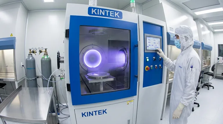
KINTEK specializes in advanced sputtering systems and lab equipment, providing the reliable tools you need for depositing complex alloys, high-melting-point metals, and uniform coatings. Our expertise ensures your laboratory operates at peak efficiency with consistent, high-purity results.
Contact our experts today to discuss your specific application and find the perfect sputtering solution for your research or production goals.
Visual Guide
Related Products
- Chemical Vapor Deposition CVD Equipment System Chamber Slide PECVD Tube Furnace with Liquid Gasifier PECVD Machine
- HFCVD Machine System Equipment for Drawing Die Nano-Diamond Coating
- RF PECVD System Radio Frequency Plasma-Enhanced Chemical Vapor Deposition RF PECVD
- 915MHz MPCVD Diamond Machine Microwave Plasma Chemical Vapor Deposition System Reactor
- Customer Made Versatile CVD Tube Furnace Chemical Vapor Deposition Chamber System Equipment
People Also Ask
- What happens during deposition chemistry? Building Thin Films from Gaseous Precursors
- What types of substrates are used in CVD to facilitate graphene films? Optimize Graphene Growth with the Right Catalyst
- Why is Chemical Vapor Deposition (CVD) equipment uniquely suited for constructing hierarchical superhydrophobic structures?
- How are carbon nanotubes grown? Master Scalable Production with Chemical Vapor Deposition
- What is plasma enhanced chemical vapor deposition PECVD equipment? A Guide to Low-Temperature Thin Film Deposition


