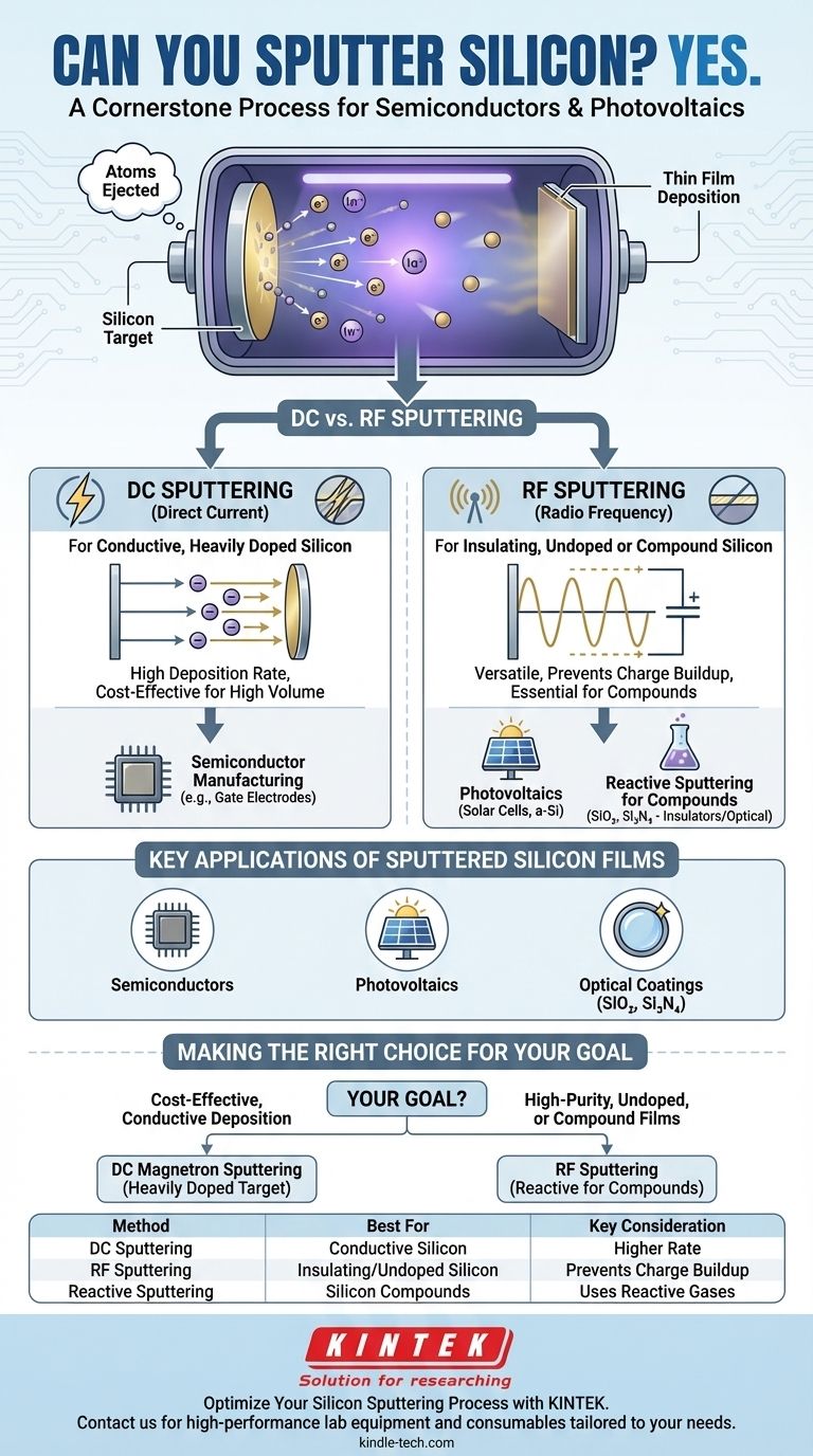
Yes, you can sputter silicon. In fact, silicon sputtering is a cornerstone process in numerous high-technology fields, including semiconductor manufacturing and photovoltaics. The technique is used to deposit thin films of pure silicon, doped silicon, and silicon compounds onto a substrate with a high degree of control.
Sputtering silicon is not only possible but is a highly mature and essential industrial process. The key consideration is choosing the correct sputtering technique—typically DC or RF—based on the electrical conductivity of the specific silicon target being used.
How Silicon Sputtering Works
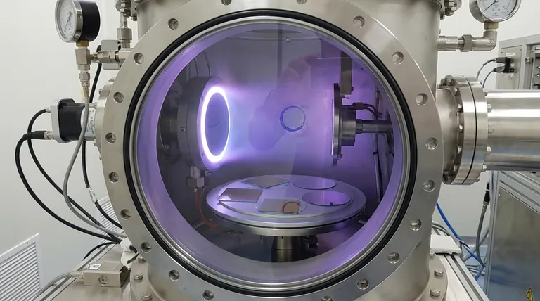
Sputter deposition is a physical vapor deposition (PVD) method. It involves bombarding a solid source material, known as a "target," with energetic ions in a vacuum, causing atoms to be ejected and deposited as a thin film onto a nearby substrate.
The Sputtering Mechanism
The process begins by creating a plasma, typically from an inert gas like argon. A strong electric field accelerates these argon ions, causing them to collide with the silicon target at high velocity.
This bombardment transfers enough momentum to knock silicon atoms loose from the target's surface. These ejected atoms then travel through the vacuum chamber and condense on the substrate, gradually building a uniform thin film.
The Critical Choice: DC vs. RF Sputtering
The primary technical decision in silicon sputtering relates to its nature as a semiconductor. The choice of power supply is critical.
DC (Direct Current) sputtering is simpler and faster. However, it only works with electrically conductive targets. Therefore, DC sputtering is suitable for heavily doped silicon (e.g., p-type or n-type) that has low resistivity.
RF (Radio Frequency) sputtering is more versatile. It uses an alternating electric field, which allows it to sputter electrically insulating or semiconducting materials. This prevents a positive charge from building up on the target surface, which would otherwise halt the process. RF sputtering is necessary for intrinsic (undoped) or lightly doped silicon.
Key Applications of Sputtered Silicon Films
Sputtered silicon films are integral to the function of many modern devices, demonstrating the process's versatility and importance.
Semiconductor Manufacturing
In microelectronics, sputtering is used to deposit thin layers of polysilicon or amorphous silicon. These layers can act as gate electrodes in transistors, as resistors, or as precursor materials that are later crystallized.
Photovoltaics (Solar Cells)
Thin-film solar cells often rely on sputtered layers of amorphous silicon (a-Si). Sputtering allows for the creation of large-area, uniform coatings on inexpensive substrates like glass or flexible plastics.
Reactive Sputtering for Compounds
The process can be extended to create silicon compounds. By introducing a reactive gas like oxygen (O2) or nitrogen (N2) into the chamber along with the argon, you can deposit silicon dioxide (SiO2) or silicon nitride (Si3N4).
These films are critical for creating insulating layers and optical coatings, such as anti-reflection layers on lenses and solar cells.
Understanding the Trade-offs
While powerful, silicon sputtering involves specific considerations that determine the outcome and efficiency of the process.
Target Conductivity Dictates the Method
As mentioned, the single most important factor is target conductivity. Using a DC power source on a high-resistivity (undoped) silicon target will fail due to charge accumulation. You must match the power supply to the material.
Deposition Rate and Cost
DC sputtering generally offers a higher deposition rate than RF sputtering, making it more cost-effective for high-volume manufacturing where conductive targets can be used. RF systems are more complex and expensive due to the need for a frequency generator and an impedance matching network.
Film Properties and Control
Sputtering parameters like gas pressure, power, and substrate temperature directly influence the properties of the resulting silicon film. These can be tuned to control the film's density, stress, crystalline structure (amorphous vs. polycrystalline), and electrical characteristics.
Making the Right Choice for Your Goal
Your application dictates the ideal sputtering method for silicon.
- If your primary focus is cost-effective deposition of conductive silicon: DC magnetron sputtering of a heavily doped silicon target is the industry standard.
- If you need to deposit high-purity, undoped, or amorphous silicon films: RF sputtering is the necessary and correct choice to handle the target's high resistivity.
- If your goal is to create insulating or optical films like SiO2 or Si3N4: Reactive sputtering with an RF power source provides the control needed to form these compound films.
Mastering these distinctions allows you to leverage sputtering to engineer silicon-based films with the precise properties your application requires.
Summary Table:
| Sputtering Method | Best For | Key Consideration |
|---|---|---|
| DC Sputtering | Conductive, heavily doped silicon | Higher deposition rate, cost-effective |
| RF Sputtering | Insulating or undoped silicon | Prevents charge buildup, versatile for compounds |
| Reactive Sputtering | Silicon compounds (SiO₂, Si₃N₄) | Uses reactive gases like O₂ or N₂ |
Optimize Your Silicon Sputtering Process with KINTEK
Whether you're developing advanced semiconductors, high-efficiency solar cells, or specialized optical coatings, choosing the right sputtering method is critical to your success. KINTEK specializes in providing high-performance lab equipment and consumables tailored to your specific silicon deposition needs.
Our experts can help you select the ideal DC or RF sputtering system to achieve precise film properties, maximize deposition rates, and control costs. We supply high-quality silicon targets—including doped and intrinsic varieties—and support reactive sputtering for compound films.
Contact us today to discuss your project requirements and discover how KINTEK's solutions can enhance your thin-film research and production. Reach out via our contact form for a personalized consultation!
Visual Guide
Related Products
- Silicon Carbide (SIC) Ceramic Sheet Flat Corrugated Heat Sink for Engineering Advanced Fine Ceramics
- Silicon Carbide (SIC) Ceramic Sheet Wear-Resistant Engineering Advanced Fine Ceramics
- Precision Machined Silicon Nitride (SiN) Ceramic Sheet for Engineering Advanced Fine Ceramics
- Silicon Carbide (SIC) Ceramic Plate for Engineering Advanced Fine Ceramics
People Also Ask
- What are the applications of silicon carbide? From Abrasives to High-Tech Semiconductors
- What is the thermal resistance of SiC? Understanding Its High Thermal Conductivity for Superior Performance
- What are the common uses of silicon carbide? Unlock Extreme Performance in Harsh Environments
- What is the temperature resistance of silicon carbide? Withstands Extreme Heat Up to 1500°C
- Why is silicon carbide more efficient? Unlock Higher Power Density with SiC's Superior Material Properties


