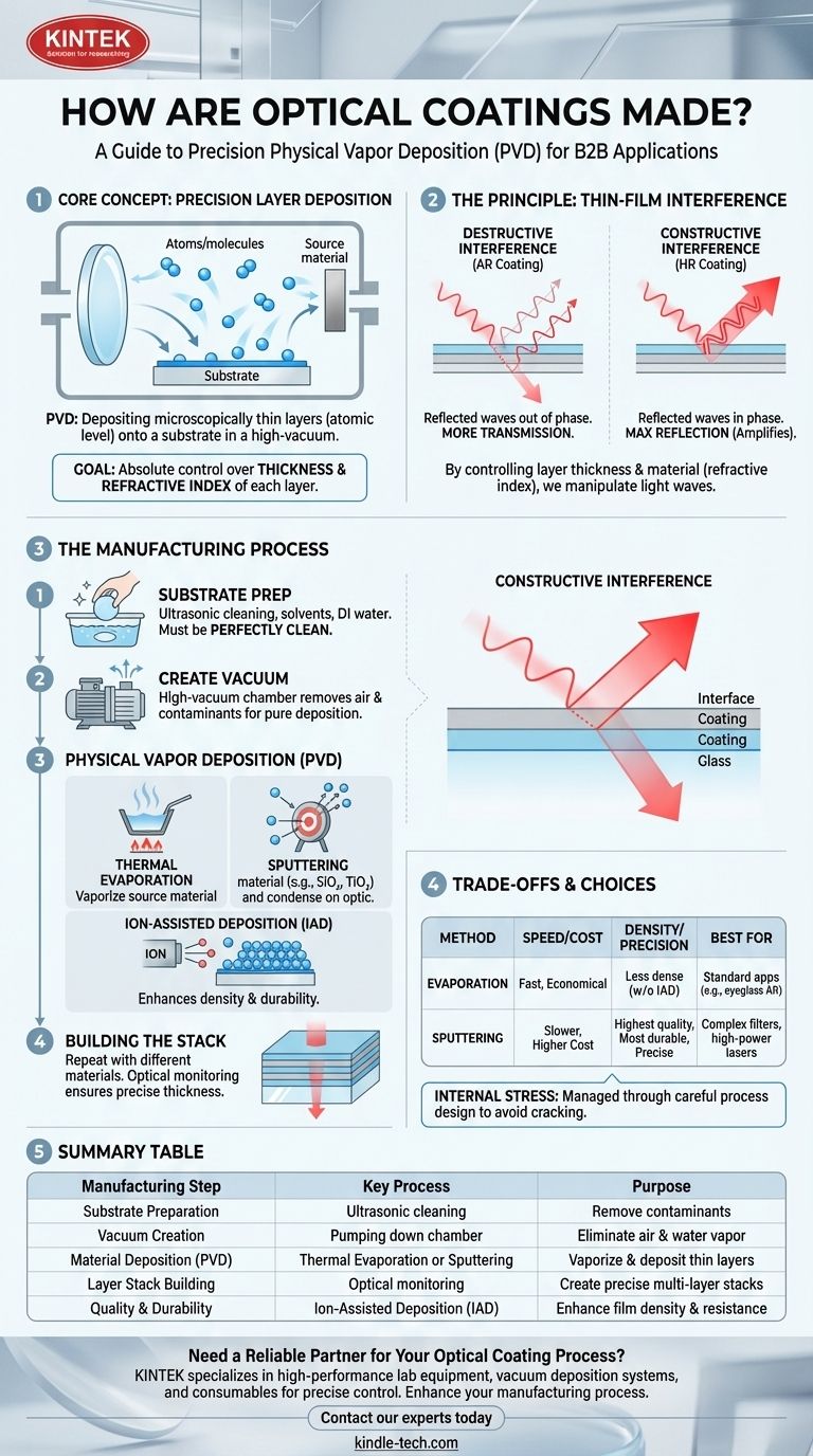
At its core, an optical coating is made by depositing microscopically thin layers of specific materials onto an optical surface, like a lens or mirror. This process, known as physical vapor deposition (PVD), takes place inside a high-vacuum chamber where materials are vaporized and then allowed to condense onto the substrate, building up a coating one atomic layer at a time. The performance of the coating is determined by creating a precise stack of multiple layers, each with a different thickness and refractive index.
The entire manufacturing process for optical coatings is engineered to achieve one fundamental goal: absolute control over the thickness and refractive index of each layer in a multi-layer stack. This precision is what allows the coating to manipulate light waves through the principle of thin-film interference.
The Principle: Why Layers Matter
Before understanding the manufacturing process, it's crucial to understand its purpose. Optical coatings work by using the wave nature of light against itself.
The Role of Thin-Film Interference
When light hits a coated surface, some of it reflects off the top of the coating, and some enters the coating, reflecting off subsequent layers or the substrate itself.
The goal is to control the phase of these reflected light waves. By precisely engineering the thickness and material (refractive index) of each layer, we can cause the reflected waves to interfere with each other.
Destructive vs. Constructive Interference
For an anti-reflection (AR) coating, the layers are designed so that the reflected waves are out of phase, causing them to cancel each other out. This is destructive interference, and it results in more light being transmitted through the optic.
For a highly-reflective (HR) mirror coating, the layers are designed to make the reflected waves perfectly in phase. This is constructive interference, which amplifies the reflection to nearly 100%.
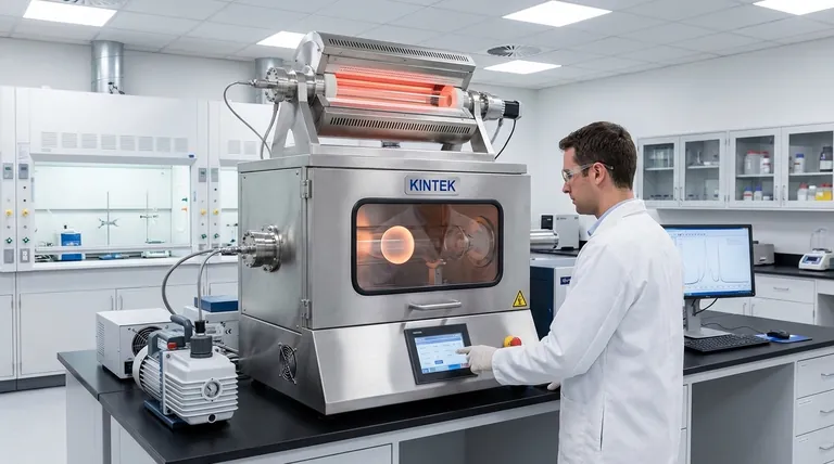
The Process: Inside the Vacuum Chamber
Creating layers that are often just a few nanometers thick requires an extremely controlled environment, free from contaminants. This is why all advanced optical coating is done in a high-vacuum chamber.
Step 1: Substrate Preparation
The optical components (substrates) must be perfectly clean. Any microscopic dust, oil, or residue will create a defect in the coating, causing it to fail. The cleaning process is a multi-stage affair involving ultrasonic baths, solvents, and deionized water.
Step 2: Creating the Vacuum
The clean substrates are loaded into a chamber, which is then pumped down to a high vacuum. This removes air and water vapor, which would otherwise contaminate the coating materials and interfere with the deposition process.
Step 3: Physical Vapor Deposition (PVD)
This is the heart of the process. A source material—typically a metal oxide or fluoride like silicon dioxide (SiO₂) or titanium dioxide (TiO₂)—is vaporized. The vaporized molecules travel in straight lines through the vacuum and condense on the relatively cool surfaces of the optics.
There are two primary methods for vaporizing the source material:
Thermal Evaporation
The source material is placed in a crucible and heated until it evaporates. This is often enhanced with an ion source (Ion-Assisted Deposition, or IAD) that bombards the substrate with energetic ions. This packs the condensing molecules more tightly, creating a denser and more durable coating.
Sputtering
A target made of the source material is bombarded with high-energy ions (usually argon). This bombardment physically knocks atoms off the target, which then "sputter" onto the substrate. Sputtering produces extremely dense, uniform, and durable films with a high degree of precision.
Step 4: Building the Stack
To create a high-performance coating, the process is repeated with different materials. A layer of a low-refractive-index material might be deposited, followed by a layer of a high-refractive-index material.
An optical monitoring system measures the light reflecting or transmitting through the optic during deposition. This allows the system to shut off the deposition source at the exact moment the layer reaches its target thickness, ensuring extreme precision.
Understanding the Trade-offs
The choice of deposition method involves a direct trade-off between performance, durability, and cost. No single process is perfect for every application.
Evaporation: Speed vs. Density
Evaporation is generally faster and less expensive than sputtering, making it suitable for many applications. However, without ion-assist, the resulting films can be less dense and more susceptible to environmental factors like humidity.
Sputtering: Precision vs. Cost
Sputtering creates the highest quality, most durable, and most repeatable coatings. Its slow, controlled nature is ideal for complex filters or high-power laser optics. This precision and durability come at the cost of longer cycle times and higher equipment expense.
Internal Stress
As layers are deposited, mechanical stress can build up within the coating. Too much stress can cause the coating to crack or delaminate from the substrate, a critical failure mode that must be managed through careful process design.
Making the Right Choice for Your Goal
The manufacturing method is directly tied to the intended use of the optic. Understanding this link is key to specifying the right product.
- If your primary focus is ultimate performance (e.g., a complex filter or low-loss AR coating): Sputtering is often the superior choice due to its exceptional layer precision and density.
- If your primary focus is durability in harsh environments (e.g., outdoor or military optics): Ion-assisted deposition or sputtering provides the dense, hard films required to resist abrasion and environmental shifts.
- If your primary focus is cost-effectiveness for standard applications (e.g., simple eyeglass AR): Thermal evaporation provides a reliable and economical solution that meets the necessary performance criteria.
Ultimately, the ability to precisely manufacture these complex, invisible structures is what transforms a simple piece of glass into a high-performance optical component.
Summary Table:
| Manufacturing Step | Key Process | Purpose |
|---|---|---|
| Substrate Preparation | Ultrasonic cleaning with solvents | Remove contaminants for defect-free coating |
| Vacuum Creation | Pumping down the chamber | Eliminate air and water vapor for pure deposition |
| Material Deposition (PVD) | Thermal Evaporation or Sputtering | Vaporize and deposit thin layers of materials |
| Layer Stack Building | Optical monitoring and repeated deposition | Create precise multi-layer stacks for interference |
| Quality & Durability | Ion-Assisted Deposition (IAD) | Enhance film density and environmental resistance |
Need a Reliable Partner for Your Optical Coating Process?
Precision optical coatings require specialized equipment and expertise. At KINTEK, we specialize in high-performance lab equipment, including vacuum deposition systems and consumables essential for creating durable anti-reflection, high-reflective, and filter coatings. Whether you are developing laser optics, consumer lenses, or complex optical filters, our solutions ensure the precise control over thickness and refractive index that your application demands.
Let us help you achieve superior optical performance and durability. Contact our experts today to discuss your specific coating challenges and explore how our reliable equipment can enhance your manufacturing process.
Visual Guide
Related Products
- HFCVD Machine System Equipment for Drawing Die Nano-Diamond Coating
- Chemical Vapor Deposition CVD Equipment System Chamber Slide PECVD Tube Furnace with Liquid Gasifier PECVD Machine
- Custom CVD Diamond Coating for Lab Applications
- Electron Beam Evaporation Coating Oxygen-Free Copper Crucible and Evaporation Boat
- Infrared Transmission Coating Sapphire Sheet Substrate Window
People Also Ask
- What types of substrates are used in CVD to facilitate graphene films? Optimize Graphene Growth with the Right Catalyst
- What is the chemical vapor deposition growth process? Build Superior Thin Films from the Atom Up
- What is the hot filament chemical vapour deposition of diamond? A Guide to Synthetic Diamond Coating
- What is the full form of HFCVD? A Guide to Hot Filament Chemical Vapor Deposition
- What is the function of tungsten filaments in HFCVD? Powering Diamond Film Synthesis with Thermal Excitation


