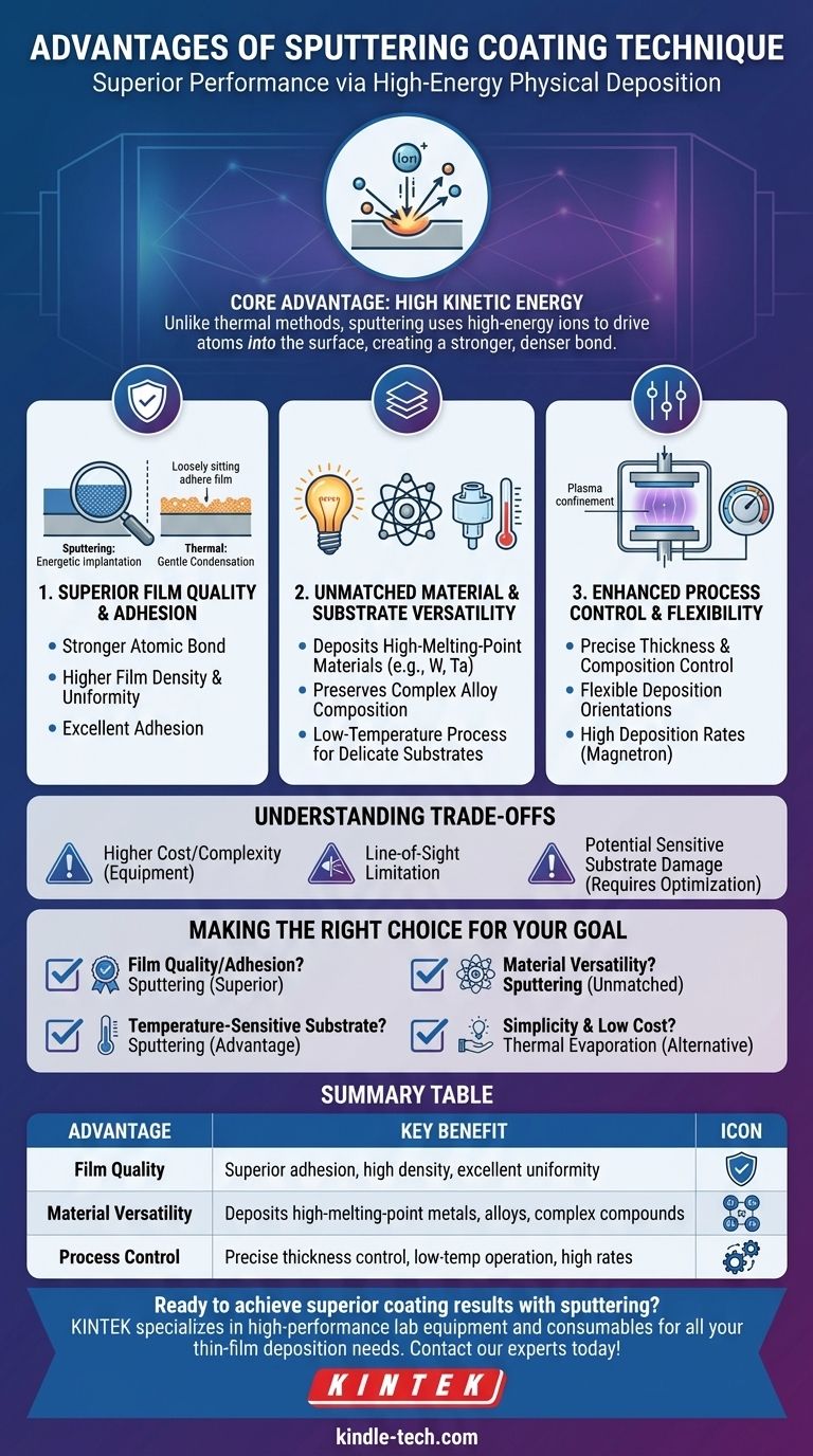
At its core, sputtering's primary advantage is its ability to produce highly adherent, dense, and uniform thin films from a vast range of materials. Unlike thermal methods that rely on melting and evaporation, sputtering is a physical process that uses high-energy ions to eject atoms from a source target, resulting in superior film quality and process versatility, even for materials with extremely high melting points.
The fundamental difference, and the source of most of its advantages, is the high kinetic energy of the sputtered atoms. This energy ensures films are not just deposited on a surface but are driven into it, creating a stronger bond and a denser, more robust final coating.
Superior Film Quality and Adhesion
The ultimate performance of a coated product often comes down to the quality of the deposited film. Sputtering excels in this area by fundamentally changing how atoms arrive at the substrate.
The Impact of High Kinetic Energy
Sputter-ejected atoms possess significantly higher kinetic energy compared to atoms from thermal evaporation. This energy is the key to creating a superior film.
Instead of gently condensing on a surface, these energetic atoms impact the substrate with force.
Exceptional Film Adhesion
This energetic bombardment results in better adhesion to the substrate. The atoms can physically implant themselves into the very near-surface region, creating a much stronger bond than methods where atoms simply rest on top.
Denser, More Uniform Films
The high energy also promotes the formation of films with higher packing densities and greater uniformity. This is crucial for applications requiring specific optical, electrical, or barrier properties.
Magnetron sputtering, a common variant, is particularly adept at achieving high uniformity over large substrate areas.
Unmatched Material and Substrate Versatility
A significant limitation of many deposition techniques is the type of materials they can handle. Sputtering overcomes many of these constraints.
Sputtering High-Melting-Point Materials
Because sputtering does not require melting the source material, it can easily deposit refractory metals and ceramics with extremely high melting points, such as tantalum or tungsten.
This is a clear advantage over thermal evaporation, which is impractical for such materials.
Depositing Complex Alloys and Mixtures
Sputtering is a physical, not chemical or thermal, transfer of material. This means it preserves the composition of the source target, making it ideal for depositing diverse mixtures and alloys with precise control.
Broad Substrate Compatibility
Sputtering is a relatively low-temperature process compared to methods like Chemical Vapor Deposition (CVD). This makes it suitable for coating temperature-sensitive materials, such as plastics or certain electronic components, without causing damage.
Enhanced Process Control and Flexibility
Beyond the film itself, the sputtering process offers a high degree of control that is essential for modern manufacturing and research.
Precise Control Over Film Properties
The process allows for highly precise control over film thickness, uniformity, and composition. This level of precision is critical for industries like semiconductors, optics, and medical devices.
Flexible Deposition Geometry
Sputtering can be performed in various orientations, including top-down. This is a distinct advantage over thermal evaporation, which can only be performed bottom-up, limiting how a substrate can be positioned and coated.
High Deposition Rates
Modern magnetron sputtering systems confine the plasma close to the target, which significantly increases the sputtering efficiency and allows for a high deposition rate, making it commercially viable for large-scale production.
Understanding the Trade-offs
No single technique is perfect for every application. To make an informed decision, it's critical to understand the potential downsides.
Process Complexity and Cost
Sputtering systems require a high-vacuum environment and a complex power supply to generate the plasma. This makes the initial equipment investment more significant than for simpler methods like thermal evaporation.
Line-of-Sight Limitation
Like evaporation, sputtering is a physical vapor deposition (PVD) method, which is generally a "line-of-sight" process. Coating highly complex, three-dimensional shapes with uniform thickness can be challenging compared to non-line-of-sight methods like CVD.
Potential for Substrate Damage
While its low-temperature nature is an advantage, the high-energy ion bombardment that gives sputtering its benefits can also cause damage to extremely sensitive substrates if the process parameters are not carefully optimized.
Making the Right Choice for Your Goal
Selecting the correct deposition method requires matching the process capabilities to your primary objective.
- If your primary focus is film quality, adhesion, and durability: Sputtering is almost always the superior choice due to the high kinetic energy of the deposited particles.
- If your primary focus is material versatility: Sputtering offers unmatched flexibility, especially for high-melting-point materials, complex alloys, and compounds.
- If your primary focus is coating temperature-sensitive substrates: Sputtering's low-temperature operation provides a significant advantage over high-temperature methods like CVD.
- If your primary focus is simplicity and low cost for a limited set of materials: A technique like thermal evaporation might be a more economical alternative.
By understanding that sputtering's core advantages stem from its energetic and physical nature, you can confidently determine when it is the optimal choice for creating high-performance coatings.
Summary Table:
| Advantage | Key Benefit |
|---|---|
| Film Quality | Superior adhesion, high density, and excellent uniformity. |
| Material Versatility | Deposits high-melting-point metals, alloys, and complex compounds. |
| Process Control | Precise thickness control, low-temperature operation, and high deposition rates. |
Ready to achieve superior coating results with sputtering? KINTEK specializes in high-performance lab equipment and consumables for all your thin-film deposition needs. Whether you're in semiconductors, optics, or medical devices, our expertise ensures you get the right solution for superior film adhesion and material versatility. Contact our experts today to discuss how we can enhance your laboratory's capabilities!
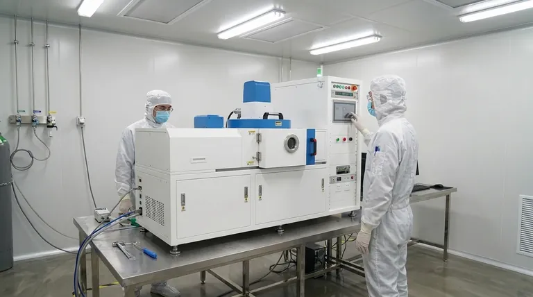
Visual Guide
Related Products
- HFCVD Machine System Equipment for Drawing Die Nano-Diamond Coating
- Infrared Transmission Coating Sapphire Sheet Substrate Window
- Electron Beam Evaporation Coating Oxygen-Free Copper Crucible and Evaporation Boat
- Custom CVD Diamond Coating for Lab Applications
- 400-700nm Wavelength Anti Reflective AR Coating Glass
People Also Ask
- What are the disadvantages and challenges of the HFCVD method? Overcome Growth Limits and Filament Issues
- What are the advantages of chemical vapor deposition? Achieve Superior Thin Films for Your Lab
- What is the chemical vapor deposition growth process? Build Superior Thin Films from the Atom Up
- Why is Chemical Vapor Deposition (CVD) equipment uniquely suited for constructing hierarchical superhydrophobic structures?
- What is the function of tungsten filaments in HFCVD? Powering Diamond Film Synthesis with Thermal Excitation


