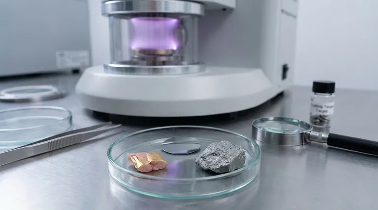
For Scanning Electron Microscopy (SEM), the most common coatings are thin layers of conductive materials such as gold (or a gold-palladium alloy), platinum, chromium, silver, and carbon. This process, known as sputter coating for metals or evaporation for carbon, is applied to non-conductive samples to make them suitable for analysis under an electron beam.
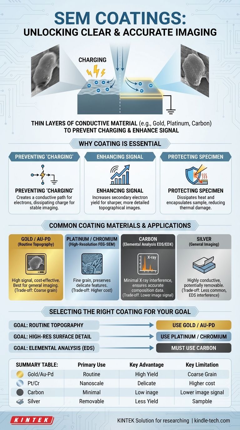
The core purpose of coating a sample for SEM is to solve a fundamental problem: an electron beam hitting a non-conductive surface creates electrical "charging," which severely distorts the image. A conductive coating provides a path for this electrical charge to ground, enabling clear, stable, and high-resolution imaging.
Why Coating is Essential for SEM Analysis
While some samples can be viewed in an SEM without preparation, most non-conductive or poorly conductive materials require a coating to produce a usable image. This preparation step addresses several key issues inherent to electron microscopy.
Preventing Electrical 'Charging'
The primary reason for coating is to improve the electrical conductivity of the specimen's surface.
When the electron beam strikes a non-conductive sample, electrons accumulate on the surface, creating a negative charge. This "charging" effect deflects the incoming beam and interferes with the emitted signals, resulting in bright patches, streaks, and distorted images.
A thin metal or carbon coating creates a conductive path, allowing excess charge to dissipate to the grounded sample holder, which stabilizes the image.
Enhancing Signal for Clearer Images
A good SEM image depends on efficiently detecting the electrons emitted from the sample.
Heavy metals like gold and platinum are excellent emitters of secondary electrons—the primary signal used for imaging surface topography. Coating a sample with one of these materials significantly increases the number of secondary electrons detected, which boosts the signal-to-noise ratio and produces a much sharper, more detailed image.
Protecting the Specimen
The high-energy electron beam can damage sensitive samples, causing structural changes or melting from localized heating.
A conductive coating helps to dissipate heat away from the area being scanned, reducing thermal damage. It also encapsulates the specimen, which can prevent beam-sensitive materials from degrading or off-gassing inside the microscope's vacuum chamber.
Common Coating Materials and Their Applications
The choice of coating material is not arbitrary; it directly impacts the quality and type of data you can acquire.
Gold and Gold-Palladium
Gold is the most common and cost-effective coating material for general-purpose SEM imaging. It has a high secondary electron yield, providing excellent signal for topographical analysis. A gold-palladium (Au/Pd) alloy is often preferred as it produces a finer grain size than pure gold, which is better for imaging at higher magnifications.
Platinum and Chromium
For very high-resolution imaging, especially with a Field Emission Gun SEM (FEG-SEM), platinum (Pt) or chromium (Cr) are superior choices. These materials can be deposited in extremely thin layers with a very fine grain structure, preserving the most delicate nanoscale surface features that a coarser gold coating might obscure.
Silver
Silver (Ag) is a highly conductive material that can be used for SEM coating. It is also sometimes chosen because it can be more easily removed from a sample after analysis compared to other metals, which is useful if the sample is needed for further testing.
Carbon
Carbon (C) is the standard coating for any analysis involving X-ray microanalysis, such as Energy-Dispersive X-ray Spectroscopy (EDS or EDX). Unlike heavy metals, carbon's X-ray signal is very low and does not interfere with the detection of elemental signals from the actual specimen, ensuring accurate compositional data.
Understanding the Trade-offs
Applying a coating is a powerful technique, but it's essential to recognize its limitations and potential downsides.
Coating Can Obscure Surface Details
Every coating adds a layer of material to your sample. If the coating is too thick or has a coarse grain structure, it can cover or alter the true nanoscale topography you are trying to observe. This is the primary trade-off between standard coatings (like gold) and high-resolution coatings (like platinum).
Interference with Elemental Analysis
This is the most critical trade-off to understand. A heavy metal coating like gold or platinum will produce strong X-ray signals of its own when struck by the electron beam. This completely masks or interferes with the elemental signals coming from your sample, making accurate compositional analysis impossible.
The Process is Destructive
Sputter coating is an irreversible process for most samples. Once a sample is coated, it is often difficult or impossible to remove the coating without altering the underlying surface.
Selecting the Right Coating for Your Goal
Your analytical goal should always dictate your choice of coating material.
- If your primary focus is routine topographical imaging: Use a gold or gold-palladium alloy for a strong, clear signal and cost-effective results.
- If your primary focus is high-resolution surface detail (FEG-SEM): Use a fine-grained material like platinum or chromium to preserve delicate nanoscale features.
- If your primary focus is elemental analysis (EDS/EDX): You must use a carbon coating to ensure your results reflect the composition of your sample, not the coating.
Choosing the correct coating transforms a challenging sample into one that yields clear, stable, and accurate analytical results.
Summary Table:
| Coating Material | Primary Use Case | Key Advantage | Key Limitation |
|---|---|---|---|
| Gold / Gold-Palladium | Routine Topographical Imaging | High secondary electron yield, cost-effective | Coarse grain can obscure fine details; interferes with EDS |
| Platinum / Chromium | High-Resolution FEG-SEM Imaging | Extremely fine grain, preserves nanoscale features | Higher cost; interferes with EDS |
| Carbon | Elemental Analysis (EDS/EDX) | Minimal X-ray interference, accurate composition data | Lower secondary electron yield for imaging |
| Silver | General Imaging (Less Common) | Highly conductive, can be removable | Less common; can interfere with EDS |
Struggling with SEM sample charging or poor image quality? The right coating is critical for success. KINTEK specializes in lab equipment and consumables, serving laboratory needs. Our experts can help you select the ideal coating materials and equipment to achieve clear, stable, and high-resolution SEM images, and ensure accurate EDS analysis. Contact us today to discuss your specific application and get a solution tailored to your lab's requirements.
Get a Consultation & Improve Your SEM Results
Visual Guide
Related Products
- Infrared Transmission Coating Sapphire Sheet Substrate Window
- Electron Beam Evaporation Coating Oxygen-Free Copper Crucible and Evaporation Boat
- Electrolytic Electrochemical Cell for Coating Evaluation
- Molybdenum Tungsten Tantalum Special Shape Evaporation Boat
People Also Ask
- What is optical coating used for? Control Light for Enhanced Performance in Your Applications
- What do optical coatings do? Control Light for Superior Optical Performance
- How do cooling jackets or heat exchangers contribute to the stability of glycerol conversion? Master Thermal Management
- How can we create a reducing environment? Master the Methods for Precise Chemical Control
- What is organic thin film? A Guide to Engineered Molecular Layers for Advanced Tech


