Knowledge What are the optical properties of thin film? Engineer Light for Anti-Reflection, Conductivity & More
Author avatar

Tech Team · Kintek Solution

Updated 6 days ago

What are the optical properties of thin film? Engineer Light for Anti-Reflection, Conductivity & More


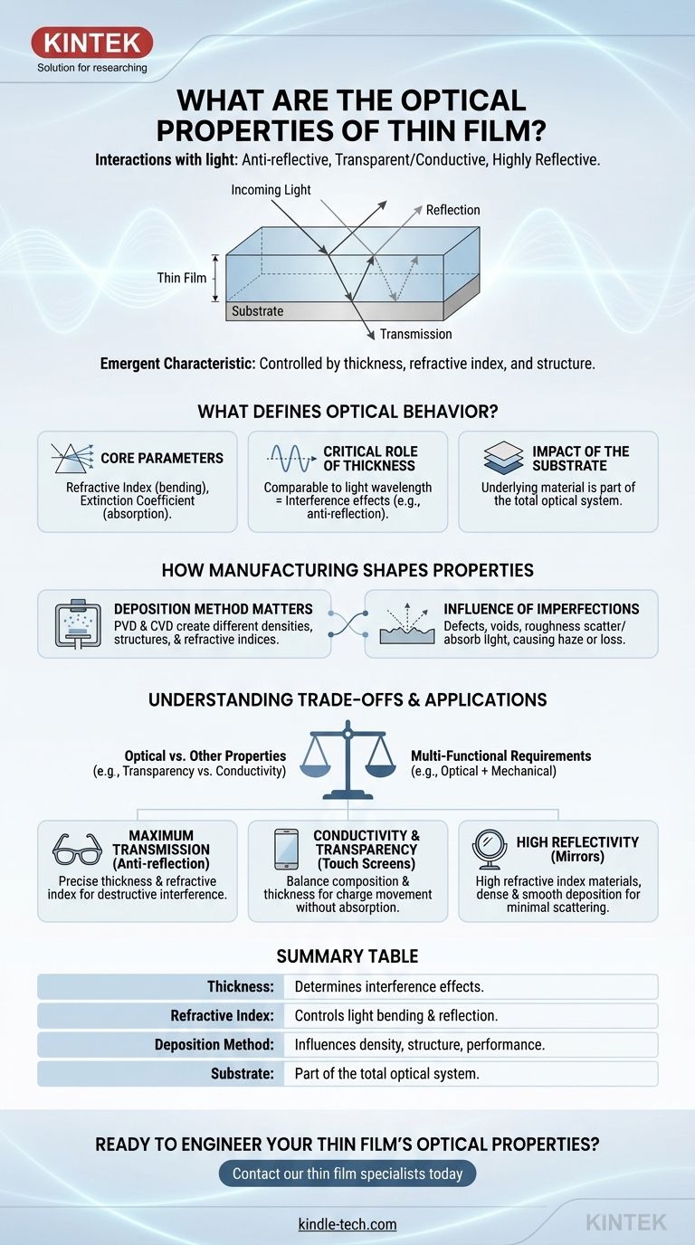
At their core, the optical properties of a thin film describe how it interacts with light, allowing it to be anti-reflective, transparent yet conductive, or highly reflective. These behaviors are not inherent to the film's material alone but are precisely controlled by its thickness, refractive index, and the presence of microscopic structural features.

The crucial takeaway is that a thin film's optical properties are an emergent characteristic, arising from a complex interplay between the chosen material, its thickness (often on the scale of light's wavelength), the underlying substrate, and the specific manufacturing process used to create it.

What are the optical properties of thin film? Engineer Light for Anti-Reflection, Conductivity & More

What Defines a Thin Film's Optical Behavior?

A thin film is a layer of material ranging from a few nanometers to several micrometers thick. When its thickness approaches the wavelength of light, its interaction with that light becomes fundamentally different from that of a bulk material.

Core Optical Parameters

The primary optical properties of any material are defined by two key parameters: refractive index and extinction coefficient. The refractive index determines how much light bends when entering the material, while the extinction coefficient measures how much light is absorbed. In thin films, these values are heavily influenced by the film's density and microstructure.

The Critical Role of Thickness

Thickness is arguably the most important factor in a thin film's optical performance. When a film's thickness is comparable to or less than the wavelength of light, interference effects between light waves reflecting from the top and bottom surfaces become dominant. This is the principle behind anti-reflection coatings on eyeglasses.

The Impact of the Substrate

A thin film is always deposited onto a substrate, and the optical properties of this underlying material are part of the total system. The difference in refractive index between the substrate, the thin film, and the surrounding air dictates how light reflects and transmits at each interface.

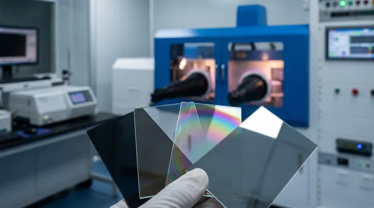
How Manufacturing Shapes Optical Properties

The method used to create a thin film has a profound and direct impact on its final optical characteristics. The same material can yield vastly different results depending on how it is deposited.

The Deposition Method Matters

Techniques like Physical Vapor Deposition (PVD) and Chemical Vapor Deposition (CVD) create films with different densities, crystal structures, and internal stresses. These microscopic variations directly alter the film's refractive index and its ability to absorb light.

The Influence of Imperfections

Real-world thin films are not perfect. Structural defects, voids, localized impurities, and surface roughness all affect optical properties. These imperfections can scatter light, leading to haze, or absorb light, reducing transmission and increasing energy loss. Roughness, in particular, has a strong effect on reflection and transmission coefficients.

Understanding the Trade-offs

Thin films are rarely designed for a single purpose. Optimizing for one property often requires a compromise in another, and understanding these balances is key to successful application.

Balancing Optical and Other Properties

A classic example is a transparent conductive oxide (TCO) used in touch screens. The film must be optically transparent to see the display, but also electrically conductive to register a touch. Increasing conductivity often involves making the film thicker or doping it more heavily, which can reduce its transparency.

Multi-Functional Requirements

Many applications demand films that meet photonic, mechanical, and chemical requirements simultaneously. A coating on a camera lens, for example, must not only be anti-reflective (optical) but also durable and scratch-resistant (mechanical).

Making the Right Choice for Your Goal

The "best" optical properties are entirely dependent on the intended application. By understanding the core principles, you can engineer a film to manipulate light for a specific outcome.

  • If your primary focus is maximum transmission (e.g., anti-reflection coatings): Your goal is to precisely control the film's thickness and refractive index to cause destructive interference for specific wavelengths of light.
  • If your primary focus is conductivity with transparency (e.g., touch screens, solar cells): You must carefully balance material composition and thickness to allow sufficient charge carrier movement without significantly absorbing visible light.
  • If your primary focus is high reflectivity (e.g., mirrors): You will choose materials with a high refractive index and deposit them with a process that yields a dense, smooth film to minimize scattering and absorption.

Ultimately, engineering a thin film's optical properties is about controlling matter at the nanoscale to precisely dictate its interaction with light.

Summary Table:

Key Factor Impact on Optical Properties
Thickness Determines light interference effects (e.g., anti-reflection).
Refractive Index Controls how much light bends and reflects at interfaces.
Deposition Method (PVD/CVD) Influences film density, structure, and final performance.
Substrate The underlying material is part of the total optical system.

Ready to Engineer Your Thin Film's Optical Properties?

The precise optical behavior of a thin film—whether for anti-reflection, transparent conductivity, or high reflectivity—is dictated by its material, thickness, and the deposition process. At KINTEK, we specialize in providing the advanced lab equipment and consumables needed to achieve exacting optical specifications for your research and production.

Let our expertise help you control light at the nanoscale. Contact our thin film specialists today to discuss your project requirements.

Visual Guide

What are the optical properties of thin film? Engineer Light for Anti-Reflection, Conductivity & More Visual Guide

Related Products

People Also Ask

Related Products

RF PECVD System Radio Frequency Plasma-Enhanced Chemical Vapor Deposition RF PECVD

RF PECVD System Radio Frequency Plasma-Enhanced Chemical Vapor Deposition RF PECVD

RF-PECVD is an acronym for "Radio Frequency Plasma-Enhanced Chemical Vapor Deposition." It deposits DLC (Diamond-like carbon film) on germanium and silicon substrates. It is utilized in the 3-12um infrared wavelength range.

Chemical Vapor Deposition CVD Equipment System Chamber Slide PECVD Tube Furnace with Liquid Gasifier PECVD Machine

Chemical Vapor Deposition CVD Equipment System Chamber Slide PECVD Tube Furnace with Liquid Gasifier PECVD Machine

KT-PE12 Slide PECVD System: Wide power range, programmable temp control, fast heating/cooling with sliding system, MFC mass flow control & vacuum pump.

Microwave Plasma Chemical Vapor Deposition MPCVD Machine System Reactor for Lab and Diamond Growth

Microwave Plasma Chemical Vapor Deposition MPCVD Machine System Reactor for Lab and Diamond Growth

Get high-quality diamond films with our Bell-jar Resonator MPCVD machine designed for lab and diamond growth. Discover how Microwave Plasma Chemical Vapor Deposition works for growing diamonds using carbon gas and plasma.

Electron Beam Evaporation Coating Oxygen-Free Copper Crucible and Evaporation Boat

Electron Beam Evaporation Coating Oxygen-Free Copper Crucible and Evaporation Boat

Electron Beam Evaporation Coating Oxygen-Free Copper Crucible enables precise co-deposition of various materials. Its controlled temperature and water-cooled design ensure pure and efficient thin film deposition.

Customer Made Versatile CVD Tube Furnace Chemical Vapor Deposition Chamber System Equipment

Customer Made Versatile CVD Tube Furnace Chemical Vapor Deposition Chamber System Equipment

Get your exclusive CVD furnace with KT-CTF16 Customer Made Versatile Furnace. Customizable sliding, rotating, and tilting functions for precise reactions. Order now!

Multi Heating Zones CVD Tube Furnace Machine Chemical Vapor Deposition Chamber System Equipment

Multi Heating Zones CVD Tube Furnace Machine Chemical Vapor Deposition Chamber System Equipment

KT-CTF14 Multi Heating Zones CVD Furnace - Precise Temperature Control and Gas Flow for Advanced Applications. Max temp up to 1200℃, 4 channels MFC mass flow meter, and 7" TFT touch screen controller.

CVD Diamond Domes for Industrial and Scientific Applications

CVD Diamond Domes for Industrial and Scientific Applications

Discover CVD diamond domes, the ultimate solution for high-performance loudspeakers. Made with DC Arc Plasma Jet technology, these domes deliver exceptional sound quality, durability, and power handling.

Split Chamber CVD Tube Furnace with Vacuum Station Chemical Vapor Deposition System Equipment Machine

Split Chamber CVD Tube Furnace with Vacuum Station Chemical Vapor Deposition System Equipment Machine

Efficient split chamber CVD furnace with vacuum station for intuitive sample checking and quick cooling. Up to 1200℃ max temperature with accurate MFC mass flowmeter control.

Cylindrical Resonator MPCVD Machine System Reactor for Microwave Plasma Chemical Vapor Deposition and Lab Diamond Growth

Cylindrical Resonator MPCVD Machine System Reactor for Microwave Plasma Chemical Vapor Deposition and Lab Diamond Growth

Learn about Cylindrical Resonator MPCVD Machine, the microwave plasma chemical vapor deposition method used for growing diamond gemstones and films in the jewelry and semi-conductor industries. Discover its cost-effective advantages over traditional HPHT methods.

Laboratory Vibratory Sieve Shaker Machine Slap Vibrating Sieve

Laboratory Vibratory Sieve Shaker Machine Slap Vibrating Sieve

KT-T200TAP is a slapping and oscillating sieving instrument for laboratory desktop use, with 300 rpm horizontal circular motion and 300 vertical slapping motions to simulate manual sieving to help sample particles pass through better.

High Purity Zinc Foil for Battery Lab Applications

High Purity Zinc Foil for Battery Lab Applications

There are very few harmful impurities in the chemical composition of zinc foil, and the surface of the product is straight and smooth; it has good comprehensive properties, processability, electroplating colorability, oxidation resistance and corrosion resistance, etc.

Metallographic Specimen Mounting Machine for Laboratory Materials and Analysis

Metallographic Specimen Mounting Machine for Laboratory Materials and Analysis

Precision metallographic mounting machines for labs—automated, versatile, and efficient. Ideal for sample prep in research and quality control. Contact KINTEK today!

Custom PTFE Teflon Parts Manufacturer Grinding Bowl

Custom PTFE Teflon Parts Manufacturer Grinding Bowl

PTFE is renowned for its exceptional chemical resistance, thermal stability, and low friction properties, making it a versatile material in various industries. The PTFE grinding bowl, specifically, finds applications where these properties are crucial.

1200℃ Split Tube Furnace with Quartz Tube Laboratory Tubular Furnace

1200℃ Split Tube Furnace with Quartz Tube Laboratory Tubular Furnace

KT-TF12 split tube furnace: high-purity insulation, embedded heating wire coils, and max. 1200C. Widely used for new materials and chemical vapour deposition.

Custom PTFE Teflon Parts Manufacturer for Air Valve Applications

Custom PTFE Teflon Parts Manufacturer for Air Valve Applications

PTFE small air valve for gas-liquid sampling and sampling bag for sample collection.

E Beam Crucibles Electron Gun Beam Crucible for Evaporation

E Beam Crucibles Electron Gun Beam Crucible for Evaporation

In the context of electron gun beam evaporation, a crucible is a container or source holder used to contain and evaporate the material to be deposited onto a substrate.

Electron Beam Evaporation Coating Conductive Boron Nitride Crucible BN Crucible

Electron Beam Evaporation Coating Conductive Boron Nitride Crucible BN Crucible

High-purity and smooth conductive boron nitride crucible for electron beam evaporation coating, with high temperature and thermal cycling performance.


Leave Your Message