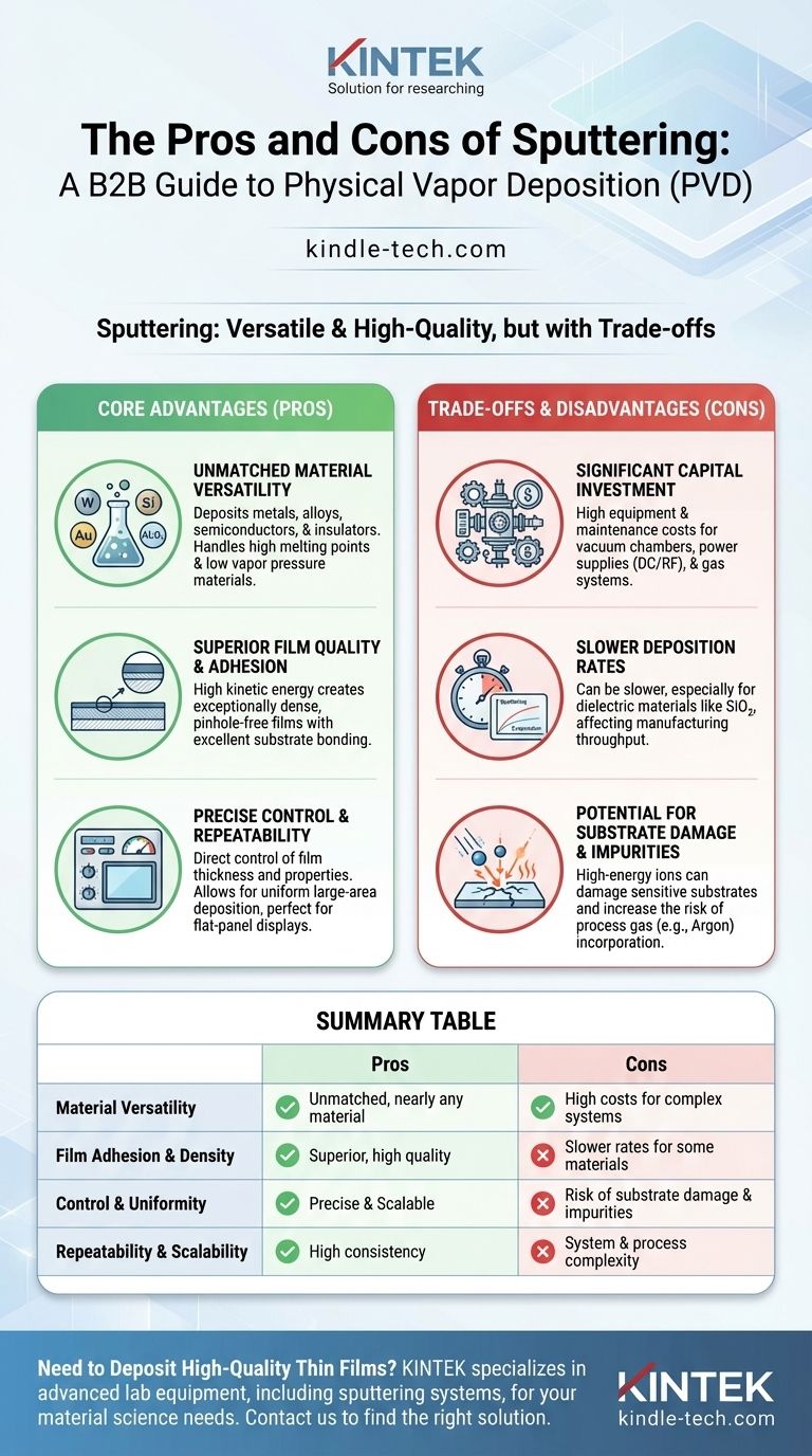
At its core, sputtering is a physical vapor deposition (PVD) process prized for its versatility and the high quality of the films it produces. The primary advantages are its ability to deposit a vast range of materials with excellent adhesion and precise control. However, these benefits come with the significant disadvantages of high equipment costs, slower deposition rates for certain materials, and the potential for substrate damage due to the high-energy nature of the process.
Sputtering offers unparalleled control and material flexibility for creating high-quality thin films. The central trade-off is accepting higher initial costs and potentially slower process times to achieve superior film adhesion, density, and purity compared to other deposition methods.
The Core Advantages of Sputtering
Sputtering's strengths lie in its ability to produce dense, well-adhered films from nearly any target material. This makes it a foundational technology in industries ranging from semiconductors to optics.
Unmatched Material Versatility
Sputtering is remarkably effective at depositing materials that are difficult or impossible to handle with other techniques like thermal evaporation.
This includes elements and compounds with extremely high melting points or low vapor pressure.
Because the process physically ejects atoms from a target rather than melting and evaporating them, almost any solid material—metals, alloys, semiconductors, and insulators—can be deposited.
Superior Film Quality and Adhesion
Atoms ejected from the sputtering target have significantly higher kinetic energy than those from an evaporation source.
This high energy results in films that are exceptionally dense, with fewer pinholes or defects.
Crucially, it also promotes excellent adhesion between the film and the substrate, sometimes forming a thin diffusion layer at the interface that creates an incredibly strong bond.
Precise Control and Repeatability
The sputtering process offers a high degree of control over the final film properties.
Film thickness is directly managed by controlling parameters like the target current and deposition time, leading to highly repeatable results from one run to the next.
This control also allows for the deposition of uniform films over very large areas, a critical requirement for manufacturing flat-panel displays, solar cells, and architectural glass.
Understanding the Trade-offs and Disadvantages
While powerful, sputtering is not a universal solution. Its disadvantages are primarily related to cost, speed, and the energetic nature of the process itself.
Significant Capital Investment
Sputtering systems are complex and require a substantial upfront investment.
The necessary components, including vacuum chambers, high-voltage power supplies (DC or RF), and gas handling systems, are expensive to purchase and maintain.
Slower Deposition Rates
Compared to a method like thermal evaporation, sputtering can be a slower process, especially for certain materials.
Dielectric materials like silicon dioxide (SiO2) are a well-known example where deposition rates are relatively low, which can impact manufacturing throughput.
Potential for Substrate Damage and Impurities
The same high-energy ions that create excellent adhesion can also cause problems.
This ionic bombardment can damage sensitive substrates, such as organic solids or some semiconductor devices. The energy transfer also leads to substrate heating, which requires careful management.
Furthermore, because sputtering operates in a lower vacuum range than evaporation, there is a slightly greater tendency to incorporate process gas atoms (like Argon) as impurities in the growing film.
System and Process Complexity
Operating a sputtering system effectively requires technical expertise.
Depositing insulating materials, for example, necessitates the use of more complex and expensive RF power supplies and impedance matching networks.
Additionally, managing the significant heat generated at the target requires an efficient cooling system to prevent damage and maintain process stability.
Is Sputtering the Right Choice for Your Application?
Choosing a deposition technique requires aligning the process capabilities with your primary goal. Sputtering excels where film quality and material choice are paramount.
- If your primary focus is high-quality, adhesive films of complex alloys or high-melting-point materials: Sputtering is almost certainly the superior choice due to its versatility and the quality of the resulting film.
- If your primary focus is high-speed, low-cost deposition of simple metals: A simpler technique like thermal evaporation may be a more cost-effective and faster solution.
- If you are working with delicate, heat-sensitive, or organic substrates: You must carefully control sputtering parameters or consider alternative, lower-energy deposition methods to avoid damaging your material.
Ultimately, sputtering is a powerful and precise tool for creating advanced materials when its trade-offs are properly managed.
Summary Table:
| Pros | Cons |
|---|---|
| Unmatched material versatility (metals, alloys, insulators) | High equipment and maintenance costs |
| Superior film adhesion and density | Slower deposition rates for some materials |
| Precise control and excellent uniformity | Potential for substrate damage from high energy |
| High repeatability and scalability | Risk of incorporating process gas impurities |
Need to Deposit High-Quality Thin Films?
Choosing the right deposition technology is critical for your R&D or production success. KINTEK specializes in providing advanced lab equipment, including sputtering systems, to meet your specific material science and thin-film application needs.
Our experts can help you determine if sputtering is the ideal solution for your project, ensuring you achieve the superior film adhesion, density, and material versatility your work demands.
Contact KINTEK today to discuss your application and discover the right equipment for your laboratory.
Visual Guide
Related Products
- Spark Plasma Sintering Furnace SPS Furnace
- Vacuum Induction Melting Spinning System Arc Melting Furnace
- Chemical Vapor Deposition CVD Equipment System Chamber Slide PECVD Tube Furnace with Liquid Gasifier PECVD Machine
- Customer Made Versatile CVD Tube Furnace Chemical Vapor Deposition Chamber System Equipment
People Also Ask
- What technical advantages does a Spark Plasma Sintering (SPS) furnace offer for LZP ceramics? Enhance Ionic Conductivity
- What is the pressure for spark plasma sintering? A Guide to Optimizing SPS Parameters
- Why are Spark Plasma Sintering (SPS) furnaces or hot presses utilized in the preparation of Li3PS4 solid electrolytes?
- What is the process fundamentals of spark plasma sintering? Achieve Rapid, High-Density Material Consolidation
- What is the theory of spark plasma sintering? A Guide to Rapid, Low-Temperature Densification


