In a business context, sputtering refers to a sophisticated manufacturing process, not a state of economic decline. It is a form of physical vapor deposition (PVD) used to apply exceptionally thin, high-performance coatings onto a product's surface. This process works on an atomic level to enhance a product's durability, functionality, or appearance.
Sputtering is not merely a production step; it is a strategic technological capability. For a business, it represents an investment in creating advanced products with superior performance, giving the company a significant competitive edge in high-tech industries like electronics, optics, and medical devices.

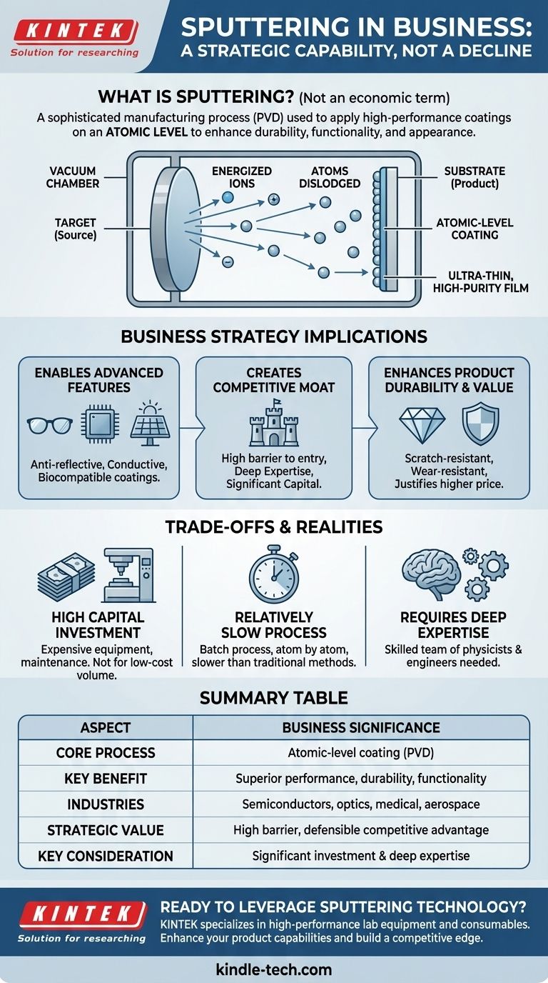
What is Sputtering? From Physics to Product
To understand its business impact, you first need a clear, non-technical picture of the process itself. Sputtering is a highly controlled technique that occurs inside a vacuum chamber.
The Core Concept: Atomic-Level Coating
Think of sputtering as a form of atomic-level sandblasting where the goal is to coat something, not erode it. Inside a vacuum, energized particles (ions) are shot at a source material, known as a target. This impact is so forceful it knocks individual atoms or molecules off the target.
These dislodged atoms then travel in a straight line and deposit themselves onto the product's surface (the substrate), building up a new layer one atom at a time.
The Result: An Ultra-Thin, High-Purity Film
The result of this process is an incredibly thin, uniform, and highly pure film. Because it is built atom by atom, the coating adheres perfectly to the substrate and can provide properties that the bulk material does not have on its own.
The Versatility: Coating Almost Anything
A key advantage of sputtering is its versatility. Unlike some other processes, it can be used to deposit a vast range of materials, including metals, alloys, ceramics, and other insulators. This allows businesses to apply conductive, reflective, or extremely hard coatings to diverse materials like glass, plastic, metal, and semiconductors.
Why Sputtering Matters for Business Strategy
A company's decision to use or invest in sputtering technology has significant strategic implications. It is often a sign of a move toward higher-value, more defensible product lines.
Enabling Advanced Product Features
Sputtering is the enabling technology behind countless modern products. For example, it is used to create anti-reflective coatings on eyeglasses and camera lenses, conductive layers in semiconductor chips and solar panels, and biocompatible coatings on medical implants.
Creating a Competitive Moat
Sputtering systems require significant capital investment and deep technical expertise to operate. This high barrier to entry means that companies with established sputtering capabilities have a strong competitive advantage that is difficult and expensive for rivals to replicate.
Enhancing Product Durability and Value
Sputtered coatings can dramatically increase a product's lifespan and perceived value. Thin films of materials like titanium nitride or diamond-like carbon create surfaces that are exceptionally resistant to scratches, wear, and corrosion, justifying a higher price point.
Understanding the Trade-offs and Business Realities
While powerful, sputtering is not a universal solution. Its strategic value is balanced by significant operational costs and complexities.
High Capital Investment
Sputtering equipment is expensive to purchase, install, and maintain. It is not a technology for low-cost, high-volume manufacturing but rather for applications where performance justifies the cost.
A Relatively Slow Process
Because it operates in a vacuum and deposits material atom by atom, sputtering is a batch process that is slower than conventional coating methods like painting or electroplating. This impacts production throughput and cost-per-unit.
Requirement for Deep Expertise
Successfully developing and running a sputtering process requires a team of highly skilled physicists and engineers. It is a knowledge-intensive capability, making talent acquisition and retention a critical factor for success.
How to Evaluate Sputtering in a Business Context
When you see the term "sputtering" in a company report or investment analysis, its significance depends entirely on the context.
- If a company is investing in sputtering capability: This signals a strategic shift toward producing higher-margin, technologically advanced products and building a defensible market position.
- If a company is a supplier of sputtering targets or equipment: This identifies them as a critical player in the high-tech supply chain for industries like semiconductors, aerospace, and optics.
- If a product's key feature relies on a sputtered coating: This means its core value is tied to a complex and expensive manufacturing process, which is both a strength (hard to copy) and a potential risk (process sensitivity, supply chain dependence).
Ultimately, understanding sputtering allows you to see beyond a product's surface and recognize the deep technological investment that drives its competitive value.
Summary Table:
| Aspect | Business Significance |
|---|---|
| Core Process | Atomic-level coating using Physical Vapor Deposition (PVD) |
| Key Benefit | Creates superior product performance, durability, and functionality |
| Industries | Semiconductors, electronics, medical devices, optics, aerospace |
| Strategic Value | High barrier to entry creates a defensible competitive advantage |
| Key Consideration | Requires significant capital investment and deep technical expertise |
Ready to leverage sputtering technology for your products? KINTEK specializes in high-performance lab equipment and consumables, including sputtering targets and deposition systems. Our expertise helps businesses in the semiconductor, medical, and optics industries enhance their product capabilities and build a competitive edge. Contact our experts today to discuss how our solutions can advance your manufacturing process.
Visual Guide