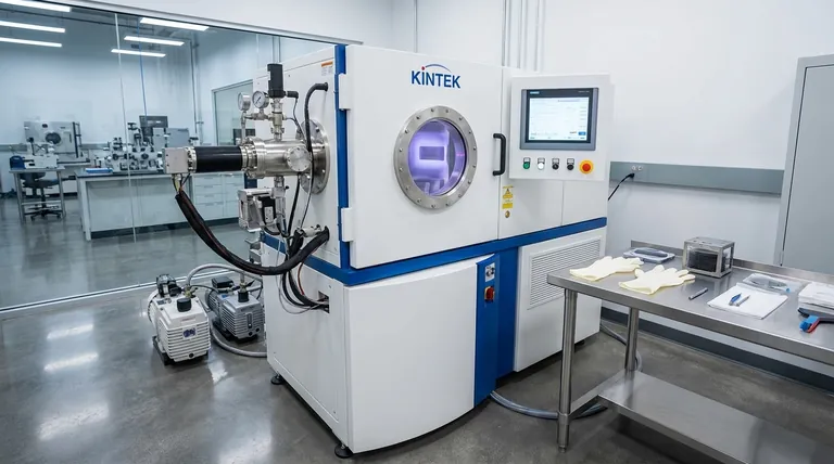
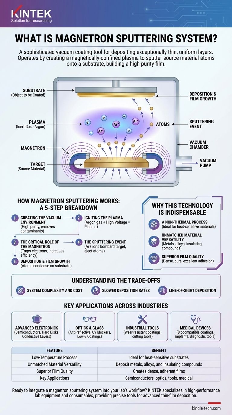
At its core, a magnetron sputtering system is a sophisticated vacuum coating tool used to deposit exceptionally thin and uniform layers of material onto a surface. It operates by creating a magnetically-confined plasma of an inert gas, such as argon. This plasma bombards a source material, known as the target, with high-energy ions, physically knocking atoms off its surface in a process called "sputtering." These ejected atoms then travel through the vacuum and condense onto a substrate, building a high-purity film atom by atom.
The true value of magnetron sputtering lies not just in its ability to create thin films, but in its precise control over a vast range of materials at low temperatures. This versatility makes it a foundational technology for manufacturing everything from semiconductor chips and advanced optics to wear-resistant tools.
How Magnetron Sputtering Works: A Step-by-Step Breakdown
To understand the system, we must first understand the process. It is a highly controlled sequence of physical events occurring within a vacuum.
Creating the Vacuum Environment
First, a vacuum chamber is pumped down to a very low pressure. This removes air and other contaminants that could react with the coating material, ensuring the final film is extremely pure.
Igniting the Plasma
A small amount of an inert gas, typically argon, is introduced into the chamber. A high voltage is then applied to the target material, causing the gas to break down and form a plasma—a glowing cloud of positive ions and free electrons.
The Critical Role of the Magnetron
This is the key to the technology. A powerful magnetic field, generated by a magnetron located behind the target, traps the free electrons near the target's surface. This dramatically increases the probability of these electrons colliding with and ionizing argon atoms, which makes the plasma far more dense and efficient.
The Sputtering Event
The positively charged argon ions in the plasma are accelerated by the electric field and smash into the negatively charged target. This physical bombardment has enough energy to eject, or "sputter," neutral atoms from the target material.
Deposition and Film Growth
The ejected target atoms travel in a straight line through the vacuum until they strike the substrate (the object to be coated). Upon arrival, they condense and build up, layer by layer, to form a dense and highly adherent thin film.
Why This Technology is Indispensable
Magnetron sputtering is not just one of many coating methods; its unique properties make it essential for applications where performance and precision are paramount.
A Non-Thermal Process
The deposition occurs without significant heating of the substrate. This is critical for coating heat-sensitive materials like plastics, complex electronics, and medical devices that would be damaged by other high-temperature methods.
Unmatched Material Versatility
The process is purely physical, not chemical. This means virtually any material can be sputtered, including metals, alloys, and even insulating compounds, making it suitable for an enormous range of applications.
Superior Film Quality
Sputtered atoms arrive at the substrate with higher kinetic energy compared to other vacuum techniques like thermal evaporation. This results in films that are incredibly dense, pure, and have superior adhesion to the substrate.
Understanding the Trade-offs
No technology is without limitations. Objectivity requires acknowledging where magnetron sputtering may not be the ideal choice.
System Complexity and Cost
Sputtering systems require a significant investment in vacuum chambers, high-voltage power supplies, and control systems. They are more complex and costly than simpler coating methods.
Slower Deposition Rates
While the magnetron enhances speed, the process is generally slower than methods like thermal evaporation. This can be a limiting factor for applications requiring very thick coatings or high-volume throughput.
Line-of-Sight Deposition
Sputtered atoms travel in a direct line from the target to the substrate. This makes it challenging to uniformly coat complex, three-dimensional shapes without sophisticated rotating fixtures for the substrate.
Key Applications Across Industries
The unique benefits of magnetron sputtering have made it a cornerstone manufacturing process in numerous high-tech fields.
- If your primary focus is advanced electronics: Sputtering is the industry standard for depositing the conductive and insulating layers in semiconductor chips and for creating the magnetic media in computer hard disks.
- If your primary focus is optics and glass: This is the preferred method for applying anti-reflective films, UV blockers, and the low-emissivity (Low-E) coatings on architectural glass that improve energy efficiency.
- If your primary focus is industrial tools and components: It is used to apply super-hard, wear-resistant coatings to cutting tools and self-lubricating films to machine parts, dramatically extending their lifespan.
- If your primary focus is medical devices: The technology creates highly pure, biocompatible coatings on implants to prevent rejection and functional layers on diagnostic tools.
Ultimately, magnetron sputtering is a pivotal technology that enables the high-performance surfaces driving innovation in nearly every advanced industry.
Summary Table:
| Feature | Benefit |
|---|---|
| Low-Temperature Process | Ideal for heat-sensitive substrates like plastics and electronics. |
| Unmatched Material Versatility | Deposit metals, alloys, and insulating compounds with high purity. |
| Superior Film Quality | Creates dense, highly adherent films with excellent uniformity. |
| Key Applications | Semiconductors, advanced optics, wear-resistant coatings, medical devices. |
Ready to integrate a magnetron sputtering system into your lab's workflow? KINTEK specializes in high-performance lab equipment and consumables, providing the precise tools you need for advanced thin-film deposition. Our expertise ensures you get a solution tailored to your specific research or production goals in semiconductors, optics, or medical device manufacturing. Contact our experts today to discuss how we can enhance your laboratory's capabilities!
Visual Guide
Related Products
- Spark Plasma Sintering Furnace SPS Furnace
- RF PECVD System Radio Frequency Plasma-Enhanced Chemical Vapor Deposition RF PECVD
People Also Ask
- What is SPS sintering method? A Guide to High-Speed, High-Performance Material Fabrication
- What are the advantages of CAMI/SPS for W-Cu composite preparation? Reduce cycles from hours to seconds.
- What is the mechanism of SPS process? A Deep Dive into Rapid, Low-Temperature Sintering
- What is the theory of spark plasma sintering? A Guide to Rapid, Low-Temperature Densification
- What is the pressure for spark plasma sintering? A Guide to Optimizing SPS Parameters

