In essence, physical sputtering is a process that ejects atoms from a solid material by bombarding it with energetic particles. Think of it as a nanoscale version of sandblasting, but instead of using sand to strip paint, it uses individual ions to knock atoms loose. These dislodged atoms then travel and deposit onto a nearby object, forming an ultra-thin, highly controlled film. This technique is a cornerstone of modern manufacturing for everything from computer chips to anti-reflective coatings on glasses.
Sputtering is not a melting or chemical process; it is a purely physical phenomenon driven by momentum transfer. This core principle is what makes it exceptionally versatile and controllable, allowing engineers to create high-quality thin films from an almost limitless range of materials.
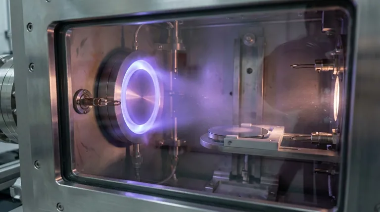
The Mechanics of Sputtering: A Nanoscale Collision
To understand sputtering, it's best to visualize it as a sequence of events occurring within a vacuum chamber. The entire process relies on creating the right conditions for a controlled, atomic-level billiard game.
Step 1: Generating the Plasma
The process begins in a high-vacuum chamber, which is backfilled with a small amount of an inert gas, most commonly argon (Ar).
A strong electric field is then applied within the chamber. This field energizes the gas, stripping electrons from the argon atoms and creating a plasma—an ionized gas consisting of positive argon ions (Ar+) and free electrons.
Step 2: Ion Bombardment
The material to be deposited, known as the target, is set up as a negative electrode (a cathode).
The positively charged argon ions in the plasma are naturally attracted to this negatively charged target. They accelerate toward it, striking its surface with tremendous kinetic energy.
Step 3: The Collision Cascade
A single incoming argon ion does not simply "chip off" a surface atom. Instead, it triggers a collision cascade beneath the surface.
The high-energy ion collides with target atoms, transferring its momentum like a cue ball striking a rack in billiards. These atoms, in turn, hit others in a chain reaction that propagates back toward the surface.
Step 4: Ejection and Deposition
If an atom near the surface receives enough momentum from this internal cascade, it can overcome the forces holding it to the target and be ejected into the vacuum. This ejected atom is what we call "sputtered."
These sputtered atoms travel in a straight line until they strike a nearby object, called the substrate. They condense on the substrate's surface, gradually building up, atom by atom, to form a thin film.
Why Sputtering is a Foundational Technique
Sputtering isn't just one option among many; for certain applications, its unique physical mechanism provides indispensable advantages over other methods like thermal evaporation.
Unmatched Material Versatility
Because sputtering is a physical momentum-transfer process, it can be used to deposit virtually any material. This includes high-melting-point metals (like tungsten or tantalum), alloys, and even insulating ceramics, which are impossible to deposit using thermal methods.
Superior Film Quality and Adhesion
Sputtered atoms arrive at the substrate with significantly higher kinetic energy (1-10 eV) compared to evaporated atoms (~0.1 eV). This extra energy allows the atoms to move around on the surface, finding optimal positions to form a denser, more uniform film.
This energy also promotes better adhesion, as the arriving atoms can implant slightly into the substrate surface, creating a much stronger bond.
Excellent Compositional Control
When sputtering a compound or alloy target (e.g., nickel-chromium), the resulting film has a composition that is extremely close to the target's. This is because the process ejects atoms based on physical collisions, not on which element evaporates more easily.
Understanding the Trade-offs and Limitations
No technique is perfect. Being an effective advisor means understanding the downsides and knowing when a different approach is better.
Slower Deposition Rates
Generally, sputtering is a slower deposition process compared to thermal evaporation. This can make it less economical for applications requiring thick films or very high throughput where ultimate film quality is not the primary concern.
System Complexity and Cost
Sputtering systems require a vacuum chamber, high-voltage power supplies, gas flow controllers, and often magnetic fields (in magnetron sputtering) to be efficient. This makes the equipment more complex and expensive to purchase and maintain than a simple thermal evaporator.
Potential for Substrate Heating
The deposition process involves more than just the sputtered atoms. The substrate is also bombarded by high-energy electrons, reflected ions, and radiation from the plasma, which can cause significant heating. This can be a problem for temperature-sensitive substrates like plastics or certain biological samples.
Risk of Gas Incorporation
A small fraction of the sputtering gas (argon) can become embedded in the growing film. While often negligible, this incorporated argon can alter the film's stress, electrical resistivity, or optical properties, which must be accounted for in high-precision applications.
Making the Right Choice for Your Goal
Selecting a deposition technique requires aligning the process capabilities with your project's primary objective.
- If your primary focus is depositing complex alloys, refractory metals, or compounds with precise composition: Sputtering is the superior choice due to its non-thermal nature and excellent stoichiometric control.
- If your primary focus is rapid, low-cost deposition of simple, low-melting-point metals: Thermal evaporation is often a more practical and economical alternative.
- If your primary focus is creating dense, highly adhesive films with specific mechanical or optical properties: Sputtering's higher-energy deposition process provides significant advantages in film quality and durability.
By understanding sputtering as a highly controlled, momentum-driven process, you can effectively leverage its unique strengths for advanced material fabrication.
Summary Table:
| Aspect | Key Takeaway |
|---|---|
| Process | Momentum transfer from energetic ions ejects atoms from a target material. |
| Primary Use | Depositing ultra-thin, highly controlled films onto a substrate. |
| Key Advantage | Unmatched material versatility and superior film adhesion/quality. |
| Common Application | Manufacturing computer chips, anti-reflective coatings, and more. |
Ready to integrate precise thin film deposition into your workflow? The experts at KINTEK are here to help. We specialize in providing high-performance lab equipment, including sputtering systems, to meet the exacting demands of research and production. Contact us today to discuss how our solutions can enhance your material fabrication processes and achieve your project goals.
Visual Guide

Related Products
- Spark Plasma Sintering Furnace SPS Furnace
- Chemical Vapor Deposition CVD Equipment System Chamber Slide PECVD Tube Furnace with Liquid Gasifier PECVD Machine
- RF PECVD System Radio Frequency Plasma-Enhanced Chemical Vapor Deposition RF PECVD
- Customer Made Versatile CVD Tube Furnace Chemical Vapor Deposition Chamber System Equipment
People Also Ask
- What are the advantages of CAMI/SPS for W-Cu composite preparation? Reduce cycles from hours to seconds.
- What is the pressure for spark plasma sintering? A Guide to Optimizing SPS Parameters
- What are the fundamentals of spark plasma sintering process? Unlock Rapid, High-Performance Material Consolidation
- What is the difference between spark plasma sintering and flash sintering? A Guide to Advanced Sintering Methods
- What technical advantages does a Spark Plasma Sintering (SPS) furnace offer for LZP ceramics? Enhance Ionic Conductivity


