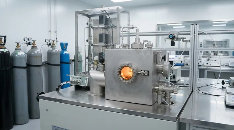
In scanning electron microscopy (SEM), sputter coating is a fundamental sample preparation technique. It involves depositing an ultra-thin, electrically conductive film, typically a metal like gold, onto a non-conducting or poorly-conducting specimen. This process is essential for preventing destructive electrical charging under the electron beam, allowing for the capture of clear, high-resolution images of the sample's surface topography.
The core purpose of sputter coating is to solve the primary challenge of imaging non-conductive materials in an SEM. By creating a conductive pathway, it grounds the sample, preventing image-distorting electrical charge and enhancing the signal needed for detailed surface analysis.
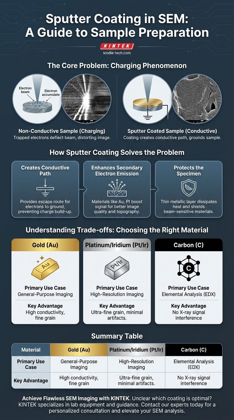
The Core Problem: Why Non-Conductive Samples Fail in SEM
The "Charging" Phenomenon
An SEM works by scanning a focused beam of electrons across a specimen. When these electrons strike a non-conductive surface, they have nowhere to go and accumulate.
This build-up of a negative static charge is known as "charging."
Distorted and Unusable Images
This trapped electrical charge deflects the incoming electron beam, severely distorting the final image. This often manifests as unnaturally bright patches, streaks, or a complete loss of fine surface detail, rendering the image unusable for serious analysis.
Potential Beam Damage
The concentrated energy from the electron beam can also physically damage delicate biological or polymeric samples, altering the very surface you intend to study.
How Sputter Coating Solves the Problem
Creating a Conductive Path
The primary function of the sputtered metallic layer is to provide an escape route for the electrons. This thin film connects the entire surface of the sample to the grounded SEM stage, preventing any charge from building up.
Enhancing Secondary Electron Emission
The materials used for coating, such as gold and platinum, are excellent emitters of secondary electrons. These electrons are the primary signal used to generate the topographic image in most SEM applications.
A good coating material boosts this signal, significantly improving the signal-to-noise ratio and the overall quality of the image.
Protecting the Specimen
The thin metallic layer also serves as a protective barrier. It helps to dissipate heat and absorb some of the energy from the primary electron beam, shielding beam-sensitive materials from damage.
Understanding the Trade-offs: Choosing the Right Material
The material you choose for coating is not arbitrary; it directly impacts your results. The goal is a uniform, fine-grained layer that conforms to the surface without obscuring it, typically between 2 and 20 nanometers thick.
Gold (Au): The General-Purpose Standard
Gold is the most common coating material due to its high conductivity, efficiency in the sputtering process, and relatively fine grain size. It is an excellent choice for general-purpose imaging.
Iridium (Ir) or Platinum (Pt): For High-Resolution Needs
For applications requiring extremely high magnification, iridium and platinum are often preferred. They can produce an even finer-grained coating than gold, which is critical for resolving nanoscale features without introducing artifacts from the coating itself.
Carbon (C): The Choice for Chemical Analysis
If your goal is to determine the elemental composition of your sample using Energy-Dispersive X-ray Spectroscopy (EDX), you must use a carbon coating.
Metals like gold produce strong X-ray peaks that will interfere with and mask the signals from the elements within your actual specimen. Carbon's low-energy signal does not create this conflict.
The Pitfall of Over-Coating
Applying too thick a layer is a common mistake. An excessively thick coating will obscure the fine surface details you are trying to observe, defeating the purpose of the analysis. The coating should be just thick enough to prevent charging.
Making the Right Choice for Your Goal
Your choice of coating material and thickness should be directly guided by your analytical objective.
- If your primary focus is high-quality surface imaging: Use a fine-grained metal like gold, platinum, or iridium to maximize conductivity and the secondary electron signal.
- If your primary focus is elemental composition analysis (EDX): Choose a carbon coating to avoid the signal interference that would mask the elements in your actual sample.
- If your primary focus is preserving delicate, nanoscale features: Use the thinnest possible coating of a very fine-grained material like iridium that successfully prevents charging.
Properly preparing your sample is not a preliminary step; it is the foundation of accurate and insightful electron microscopy.
Summary Table:
| Coating Material | Primary Use Case | Key Advantage |
|---|---|---|
| Gold (Au) | General-purpose imaging | High conductivity, fine grain |
| Platinum/Pt (Ir) | High-resolution imaging | Ultra-fine grain, minimal artifacts |
| Carbon (C) | Elemental analysis (EDX) | No X-ray signal interference |
Achieve flawless SEM imaging with the right sputter coating solution. Unclear which coating material or thickness is optimal for your specific sample? KINTEK specializes in lab equipment and consumables, serving laboratory needs with expert guidance on sputter coaters and materials. Our team can help you select the perfect setup to prevent charging, enhance signal quality, and protect delicate specimens. Contact our experts today for a personalized consultation and elevate your SEM analysis.
Visual Guide
Related Products
- Infrared Transmission Coating Sapphire Sheet Substrate Window
- Electron Beam Evaporation Coating Oxygen-Free Copper Crucible and Evaporation Boat
- 400-700nm Wavelength Anti Reflective AR Coating Glass
- Custom CVD Diamond Coating for Lab Applications
- Molybdenum Tungsten Tantalum Special Shape Evaporation Boat
People Also Ask
- What is the thinnest coating? Unlocking Unique Properties at the Atomic Scale
- What is the optical coating? Master Light Control for Superior Optical Performance
- Why do we need optical coating? To Control Light and Enhance Optical Performance
- How can we create a reducing environment? Master the Methods for Precise Chemical Control
- How do cooling jackets or heat exchangers contribute to the stability of glycerol conversion? Master Thermal Management


