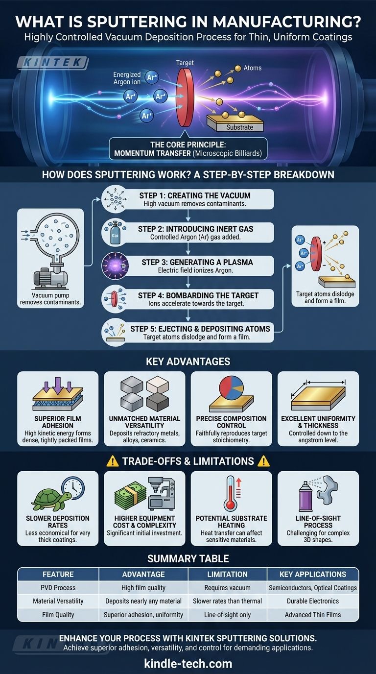
In manufacturing, sputtering is a highly controlled vacuum deposition process used to apply exceptionally thin and uniform coatings of material onto a surface. It operates not by melting, but by physically ejecting atoms from a source material (a "target") using energetic ion bombardment, which then deposit onto a substrate to form a film. This method is a cornerstone of modern high-technology industries, from semiconductors to optical lenses.
The core principle of sputtering is a momentum transfer process, akin to a microscopic game of billiards. It uses energized gas ions to physically knock atoms off a target, providing unparalleled control over film thickness, adhesion, and composition for a vast range of materials.
How Does Sputtering Work? A Step-by-Step Breakdown
To understand sputtering, it's best to visualize the process inside the deposition chamber. It is a type of Physical Vapor Deposition (PVD), meaning the material transitions from a solid to a vapor phase through purely physical means.
Step 1: Creating the Vacuum
First, a high vacuum is created within a sealed chamber. This is critical to remove air and other contaminants that could react with the coating material or interfere with the process.
Step 2: Introducing an Inert Gas
A small, precisely controlled amount of an inert gas, almost always Argon (Ar), is then introduced into the chamber. Argon is chosen because it is chemically non-reactive and has a suitable atomic mass.
Step 3: Generating a Plasma
A strong electric field is applied within the chamber, often using a high DC or RF voltage. This energy strips electrons from the Argon atoms, ionizing the gas and creating a glowing, electrically charged state of matter known as plasma.
Step 4: Bombarding the Target
The source material to be deposited, known as the target, is given a strong negative electrical charge. This causes the positively charged Argon ions (Ar+) from the plasma to accelerate violently towards the target, like a magnet pulling on a piece of iron.
Step 5: Ejecting and Depositing Atoms
When these high-energy Argon ions collide with the target, they transfer their momentum and physically knock atoms or molecules loose from the target's surface. This ejection of material is the "sputtering" event. These dislodged atoms travel through the chamber and condense on the substrate (the object being coated), building up a thin, uniform film.
Key Advantages of the Sputtering Process
Sputtering is not chosen for its speed, but for its precision and versatility. Its unique characteristics offer significant benefits for advanced manufacturing.
Superior Film Adhesion
Sputtered atoms arrive at the substrate with significantly more kinetic energy than atoms from other methods like thermal evaporation. This energy helps them form a denser, more tightly packed film with exceptional adhesion to the surface.
Unmatched Material Versatility
Because sputtering is a physical rather than a thermal process, it is not limited by a material's melting point. This allows for the deposition of a vast range of materials, including refractory metals (like tungsten and tantalum), alloys, and even ceramics and other compounds.
Precise Control Over Composition
Sputtering faithfully reproduces the composition of the source target in the deposited film. This is crucial for depositing complex alloys, as the components are ejected together without the separation that can occur in melting-based processes where different elements have different evaporation rates.
Excellent Uniformity and Thickness Control
By carefully managing parameters like gas pressure, power, and deposition time, sputtering can produce films with highly uniform thickness across large areas, often controlled down to the single-angstrom level.
Understanding the Trade-offs and Limitations
No process is perfect. An objective evaluation requires acknowledging the limitations of sputtering.
Slower Deposition Rates
Generally, sputtering is a much slower process compared to thermal evaporation. This makes it less economical for applications requiring very thick coatings (many microns).
Higher Equipment Cost and Complexity
Sputtering systems require sophisticated vacuum chambers, high-voltage power supplies, cooling systems, and process controls. The initial capital investment is significantly higher than for simpler coating methods.
Potential for Substrate Heating
The constant bombardment of energetic particles can transfer a significant amount of heat to the substrate. This can be a major issue for coating heat-sensitive materials like plastics or certain biological samples, requiring specialized substrate cooling.
Line-of-Sight Process
Like spraying paint from a can, sputtering is a "line-of-sight" technique. It is challenging to uniformly coat complex, three-dimensional shapes without incorporating elaborate substrate rotation and tilting mechanisms.
Making the Right Choice for Your Application
Choosing a deposition method depends entirely on the required properties of the final film.
- If your primary focus is high-performance optical coatings: Sputtering is ideal for its ability to create dense, uniform, and precisely controlled multi-layer films for anti-reflection coatings, mirrors, and filters.
- If your primary focus is durable microelectronic components: The excellent adhesion and ability to deposit a wide variety of conductive, resistive, and dielectric layers make sputtering a standard for manufacturing semiconductors and sensors.
- If your primary focus is depositing complex alloys or refractory metals: Sputtering is the superior choice because it preserves the material's stoichiometry and is not limited by extremely high melting points.
- If your primary focus is rapid, thick, or purely decorative coatings: You might consider alternative methods like thermal evaporation or electroplating, which can offer higher deposition rates and lower equipment costs.
Ultimately, sputtering provides a level of precision and material flexibility that is essential for creating the advanced thin films that power modern technology.
Summary Table:
| Feature | Advantage | Limitation |
|---|---|---|
| Process Type | Physical Vapor Deposition (PVD) | Requires high vacuum and complex equipment |
| Material Versatility | Can deposit metals, alloys, ceramics, and compounds | Slower deposition rates than thermal methods |
| Film Quality | Superior adhesion, uniformity, and precise thickness control | Line-of-sight process; challenging for complex 3D shapes |
| Key Applications | Semiconductors, optical coatings, durable electronics | Higher initial equipment cost and potential substrate heating |
Ready to enhance your manufacturing process with precision sputtering solutions? KINTEK specializes in advanced lab equipment and consumables for thin-film deposition, serving industries from semiconductors to optics. Our expertise ensures you achieve superior film adhesion, material versatility, and exact thickness control for your most demanding applications. Contact us today to discuss how our sputtering systems can meet your specific laboratory needs and drive your innovation forward.
Visual Guide
Related Products
- Spark Plasma Sintering Furnace SPS Furnace
- Vacuum Induction Melting Spinning System Arc Melting Furnace
- Chemical Vapor Deposition CVD Equipment System Chamber Slide PECVD Tube Furnace with Liquid Gasifier PECVD Machine
- Customer Made Versatile CVD Tube Furnace Chemical Vapor Deposition Chamber System Equipment
People Also Ask
- What is the theory of spark plasma sintering? A Guide to Rapid, Low-Temperature Densification
- What is the pressure for spark plasma sintering? A Guide to Optimizing SPS Parameters
- What are the advantages of CAMI/SPS for W-Cu composite preparation? Reduce cycles from hours to seconds.
- What technical advantages does a Spark Plasma Sintering (SPS) furnace offer for LZP ceramics? Enhance Ionic Conductivity
- What are the fundamentals of spark plasma sintering process? Unlock Rapid, High-Performance Material Consolidation


