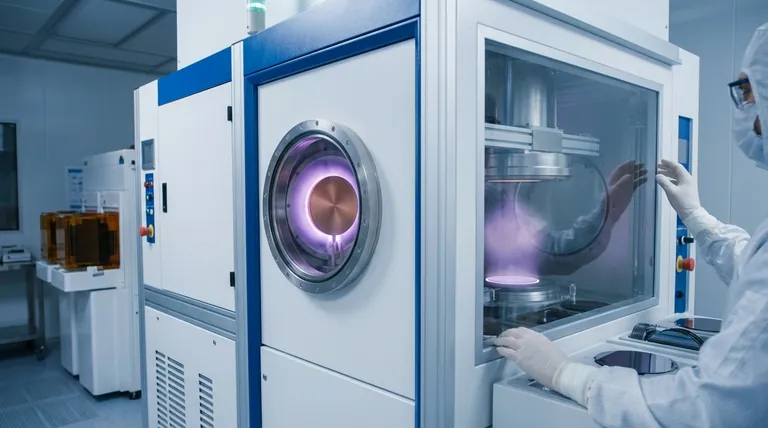
In semiconductor manufacturing, sputtering is a fundamental process of Physical Vapor Deposition (PVD) used to create ultra-thin films of material with atomic-level precision. It functions like a microscopic sandblaster, where a source material, known as a target, is bombarded with high-energy ions from a plasma. This collision physically knocks atoms off the target, which then travel through a vacuum and deposit onto a substrate, such as a silicon wafer, forming a uniform coating.
Sputtering is not a chemical reaction but a physical process of atomic-scale transfer. It uses energized ions to knock atoms from a source material, which then travel and build a precise, uniform thin film on a semiconductor wafer—a crucial step for building the circuitry in microchips.
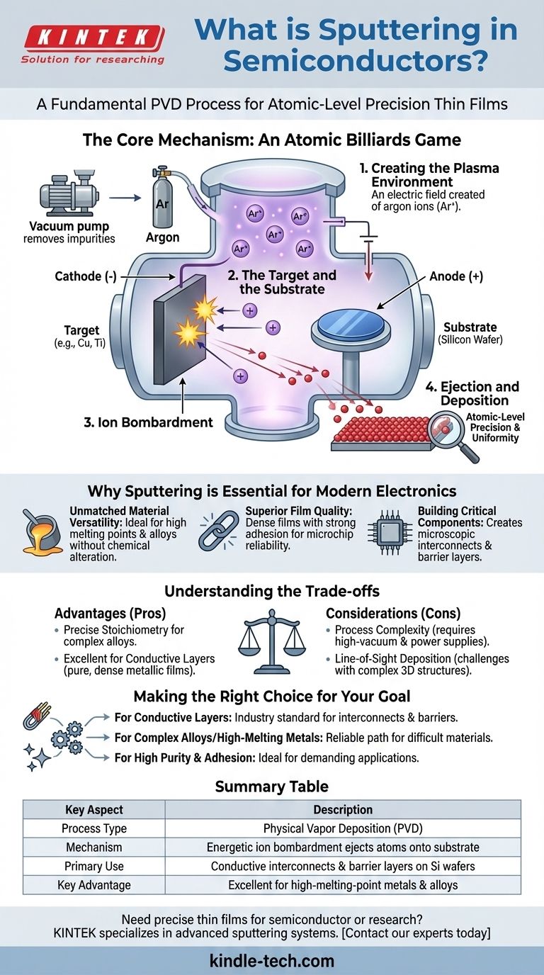
The Core Mechanism: An Atomic Billiards Game
Sputtering takes place inside a highly controlled vacuum chamber. The entire process can be understood as a sequence of physical events, much like a game of billiards at the atomic level.
Creating the Plasma Environment
First, the chamber is evacuated to a very high vacuum to remove any impurities. Then, an inert gas, most commonly argon, is introduced at a low pressure. An electric field is applied, which energizes the argon gas and strips electrons from the argon atoms, creating a glowing, ionized gas known as plasma.
The Target and the Substrate
Inside the chamber are two key components: the target and the substrate. The target is a slab of the pure material you wish to deposit (e.g., tantalum, copper, titanium). The substrate is the object you are coating, which in semiconductor fabrication is typically a silicon wafer.
Ion Bombardment
The target is given a negative electrical charge (acting as a cathode). This attracts the positively charged argon ions from the plasma, causing them to accelerate and collide with the target's surface with tremendous force.
Ejection and Deposition
This high-energy impact physically dislodges, or "sputters," atoms from the target material. These ejected atoms fly off in various directions and eventually condense on the cooler surface of the substrate, slowly building up a thin film one atom at a time.
Why Sputtering is Essential for Modern Electronics
Sputtering isn't just one option among many; it is often the best or only method for creating certain critical layers in a microchip. Its advantages stem directly from its physical nature.
Unmatched Material Versatility
Because sputtering physically knocks atoms loose rather than melting or evaporating them, it is ideal for depositing materials with extremely high melting points. It also excels at depositing alloys, as it can transfer the material from the target to the substrate without altering its chemical composition.
Superior Film Quality
The sputtered atoms arrive at the substrate with significant kinetic energy. This results in films that are very dense and adhere strongly to the underlying layer, which is critical for the reliability of a microchip.
Building Critical Components
This process is used to create essential parts of an integrated circuit. This includes the microscopic metal wires (interconnects) that carry signals and power, as well as the barrier layers that prevent different materials from mixing.
Understanding the Trade-offs
Like any engineering process, sputtering involves specific advantages and considerations that make it suitable for certain applications over others, such as Chemical Vapor Deposition (CVD).
Advantage: Precise Stoichiometry
For complex materials like alloys, sputtering faithfully reproduces the composition of the target on the substrate. This is a significant advantage over chemical or thermal methods that can struggle to maintain the correct ratio of elements.
Advantage: Excellent for Conductive Layers
Sputtering is a dominant method for depositing the metal layers that form the wiring on a chip. Its ability to create pure, dense, and uniform metallic films is unmatched for this purpose.
Consideration: Process Complexity
Sputtering systems require sophisticated high-vacuum pumps and high-voltage power supplies. This makes the equipment and process more complex than some alternatives.
Consideration: Line-of-Sight Deposition
Because sputtered atoms travel in relatively straight lines, the process can have difficulty uniformly coating highly complex, three-dimensional structures. The "shadows" cast by tall features can lead to thinner coverage in trenches or on sidewalls.
Making the Right Choice for Your Goal
Sputtering is chosen when the physical properties and purity of the deposited film are paramount. Its role is defined by its unique capabilities in handling a wide range of materials.
- If your primary focus is depositing conductive layers: Sputtering is the industry standard for creating the metal interconnects and barrier layers that form a chip's wiring.
- If your primary focus is working with complex alloys or high-melting-point metals: Sputtering provides a reliable path to create thin films from materials that are difficult to deposit using thermal or chemical methods.
- If your primary focus is achieving high purity and strong adhesion: The controlled vacuum environment and energetic nature of sputtering make it ideal for applications demanding pristine, durable films.
Ultimately, sputtering is the foundational tool that gives engineers the precise physical control needed to build the microscopic structures of modern integrated circuits.
Summary Table:
| Key Aspect | Description |
|---|---|
| Process Type | Physical Vapor Deposition (PVD) |
| Mechanism | Energetic ions bombard a target, ejecting atoms that deposit on a substrate |
| Primary Use | Creating conductive interconnects and barrier layers on silicon wafers |
| Key Advantage | Excellent for high-melting-point metals and alloys, with strong film adhesion |
| Key Consideration | Line-of-sight deposition can challenge coating complex 3D structures |
Need to deposit precise, high-quality thin films for your semiconductor or research application? KINTEK specializes in advanced lab equipment, including sputtering systems, to meet your specific material deposition needs. Our expertise ensures you get the right solution for creating reliable, high-performance layers. Contact our experts today to discuss how we can support your laboratory's goals!
Visual Guide
Related Products
- Spark Plasma Sintering Furnace SPS Furnace
- Vacuum Induction Melting Spinning System Arc Melting Furnace
- Chemical Vapor Deposition CVD Equipment System Chamber Slide PECVD Tube Furnace with Liquid Gasifier PECVD Machine
- Customer Made Versatile CVD Tube Furnace Chemical Vapor Deposition Chamber System Equipment
- HFCVD Machine System Equipment for Drawing Die Nano-Diamond Coating
People Also Ask
- What is the difference between spark plasma sintering and flash sintering? A Guide to Advanced Sintering Methods
- What is the theory of spark plasma sintering? A Guide to Rapid, Low-Temperature Densification
- What is SPS sintering method? A Guide to High-Speed, High-Performance Material Fabrication
- Why are Spark Plasma Sintering (SPS) furnaces or hot presses utilized in the preparation of Li3PS4 solid electrolytes?
- What are the advantages of CAMI/SPS for W-Cu composite preparation? Reduce cycles from hours to seconds.


