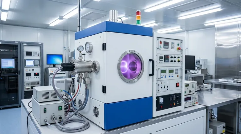
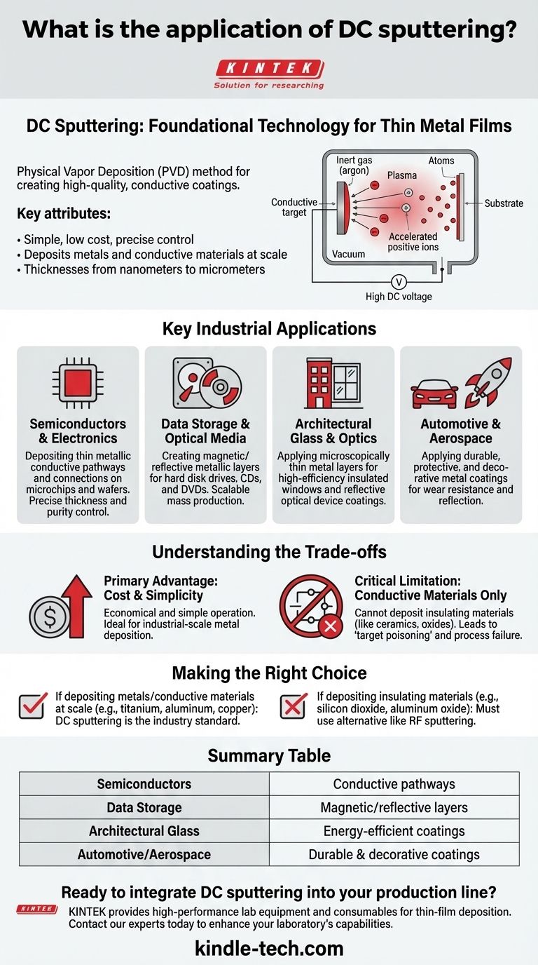
In short, DC sputtering is a foundational technology for applying thin metal films. It is a physical vapor deposition (PVD) method widely used across industries like semiconductors, optics, and data storage to create high-quality, conductive coatings. Its primary application is the cost-effective deposition of metals and other electrically conductive materials onto various substrates, ranging in thickness from a few nanometers to several micrometers.
DC sputtering's value lies in its simplicity, low cost, and precise control, making it the go-to method for depositing conductive thin films at scale. However, its reliance on a direct current means it is fundamentally limited to materials that can conduct electricity.
How DC Sputtering Works as a Deposition Tool
The Core Mechanism: Target to Substrate
DC sputtering is a type of Physical Vapor Deposition (PVD). The process takes place inside a vacuum chamber filled with an inert gas, such as argon.
A high DC voltage is applied to the material you wish to deposit, known as the "target." This voltage ionizes the gas, creating plasma.
The positive gas ions are accelerated toward the negative target, striking it with enough force to dislodge, or "sputter," atoms from its surface. These ejected atoms then travel through the chamber and condense onto the object being coated (the "substrate"), forming a thin, uniform film.
The Critical Role of Direct Current
The use of a Direct Current (DC) power source is what makes the process simple, reliable, and inexpensive. The steady voltage efficiently creates and sustains the plasma required for sputtering.
However, this requires the target material itself to be electrically conductive. A conductive target is necessary to complete the electrical circuit and prevent a buildup of positive charge that would otherwise repel the ions and stop the sputtering process.
Key Industrial Applications
The unique advantages of DC sputtering—low cost, speed, and high film quality—make it a cornerstone of manufacturing in several high-tech sectors.
Semiconductors and Electronics
In semiconductor fabrication, DC sputtering is used to deposit the thin metallic layers that form conductive pathways and connections on microchips and wafers. The process offers the precise control over film thickness and purity required for modern electronics.
Data Storage and Optical Media
The production of hard disk drives, CDs, and DVDs relies heavily on DC sputtering. It is used to lay down the magnetic or reflective metallic layers that store data. The scalability and low cost of the technique are perfect for this type of mass production.
Architectural Glass and Optics
DC magnetron sputtering is used to apply microscopically thin metal layers onto glass for high-efficiency insulated windows. These coatings reflect infrared radiation, improving thermal insulation without impacting visibility. It is also used for coatings on binoculars, telescopes, and other optical devices.
Automotive and Aerospace
In the automotive and aerospace industries, DC sputtering is used for both functional and decorative coatings. It can apply durable, protective metal films that resist wear and corrosion or create reflective surfaces for lighting components.
Understanding the Trade-offs
No single technology is perfect for every scenario. Understanding the limitations of DC sputtering is crucial for making an informed decision.
The Primary Advantage: Cost and Simplicity
The main driver for using DC sputtering is economics. DC power supplies are significantly less expensive and easier to operate than the alternatives, like Radio Frequency (RF) systems. For industrial-scale metal deposition, it is the most efficient and economical choice.
The Critical Limitation: Conductive Materials Only
The single greatest limitation of DC sputtering is its inability to deposit insulating (dielectric) materials. If you attempt to sputter a non-conductive target like a ceramic or an oxide, positive charge quickly accumulates on its surface. This buildup, known as "target poisoning," repels the incoming gas ions and extinguishes the plasma, halting the process.
Deposition Rate and Adhesion
For metals, DC sputtering typically offers a fast and controllable deposition rate. The resulting films are dense and exhibit excellent adhesion to the substrate, making them highly durable for demanding applications.
Making the Right Choice for Your Goal
Your choice between DC sputtering and other methods hinges entirely on your target material and production goals.
- If your primary focus is depositing metals or other conductive materials (like titanium, aluminum, or copper) at scale: DC sputtering is the industry standard due to its low cost, high speed, and simplicity.
- If your primary focus is depositing insulating materials (like silicon dioxide or aluminum oxide): You must use an alternative like RF (Radio Frequency) sputtering, as a DC current cannot be sustained with a non-conductive target.
Understanding this fundamental distinction between conductive and non-conductive targets is the key to leveraging sputtering technology effectively.
Summary Table:
| Application Area | Key Use of DC Sputtering |
|---|---|
| Semiconductors | Depositing conductive pathways on microchips and wafers. |
| Data Storage | Creating magnetic/reflective layers for hard drives and optical media. |
| Architectural Glass | Applying energy-efficient, reflective coatings on windows. |
| Automotive/Aerospace | Applying durable, protective, and decorative metal coatings. |
Ready to integrate DC sputtering into your production line?
KINTEK specializes in providing high-performance lab equipment and consumables for all your thin-film deposition needs. Whether you are scaling up semiconductor production or developing new optical coatings, our expertise ensures you get the right solution for depositing conductive materials efficiently and cost-effectively.
Contact our experts today to discuss how our sputtering systems can enhance your laboratory's capabilities and drive your projects forward.
Visual Guide
Related Products
- Spark Plasma Sintering Furnace SPS Furnace
- Vacuum Induction Melting Spinning System Arc Melting Furnace
- Circulating Water Vacuum Pump for Laboratory and Industrial Use
People Also Ask
- What is the theory of spark plasma sintering? A Guide to Rapid, Low-Temperature Densification
- What are the fundamentals of spark plasma sintering process? Unlock Rapid, High-Performance Material Consolidation
- What is the difference between spark plasma sintering and flash sintering? A Guide to Advanced Sintering Methods
- What is the pressure for spark plasma sintering? A Guide to Optimizing SPS Parameters
- What is the mechanism of SPS process? A Deep Dive into Rapid, Low-Temperature Sintering


