At their core, both Sputtering and Pulsed Laser Deposition (PLD) are Physical Vapor Deposition (PVD) techniques used to create thin films. The fundamental difference lies in how they generate a vapor from a source material. Sputtering uses energetic ion bombardment to physically knock atoms off a target, while PLD uses a high-power laser to ablate, or vaporize, material from the target's surface.
The choice between sputtering and PLD is a classic engineering trade-off. Sputtering is the scalable industrial workhorse for uniform coatings, while PLD is the high-precision laboratory tool for complex materials where preserving chemical composition is paramount.
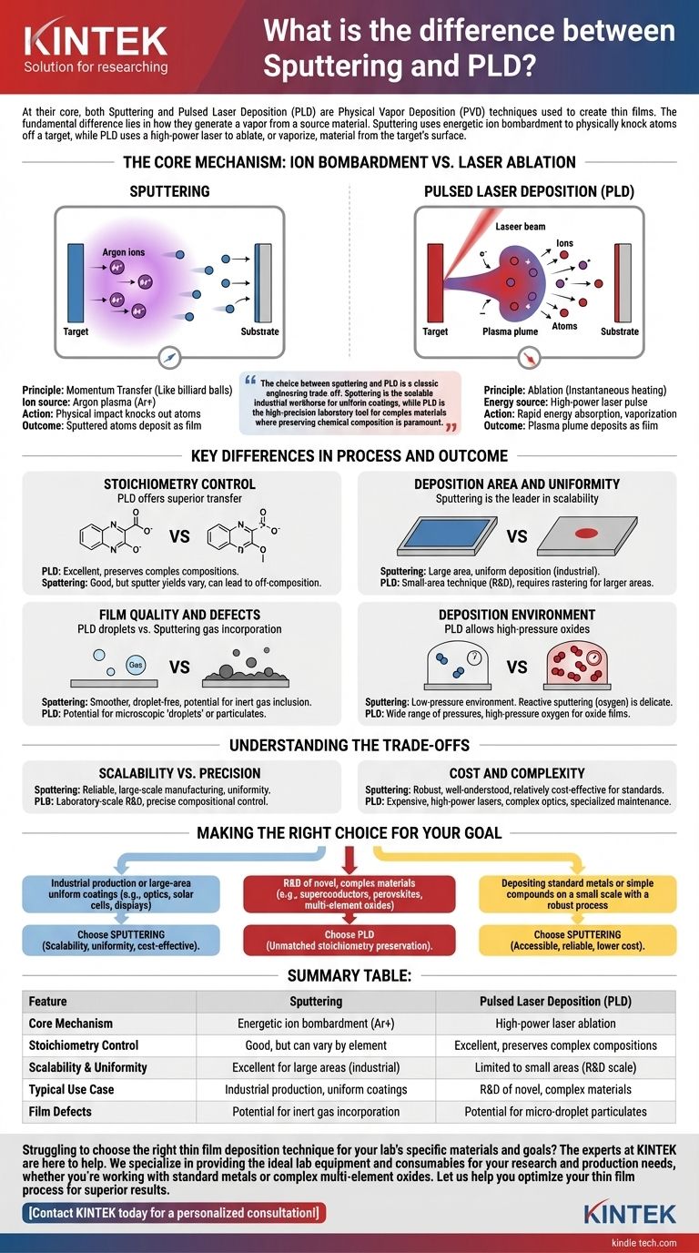
The Core Mechanism: Ion Bombardment vs. Laser Ablation
Both methods exist to solve the same problem: moving atoms from a solid source material (the "target") onto a component (the "substrate") in a vacuum. The energy source used to accomplish this defines their capabilities.
How Sputtering Works
Sputtering operates on the principle of momentum transfer, much like a cue ball breaking a rack of billiard balls.
First, a vacuum chamber is filled with a small amount of an inert gas, typically Argon. An electric field is applied, which strips electrons from the Argon atoms, creating a glowing plasma of positively charged Argon ions (Ar+).
These ions are accelerated towards the negatively charged target material. Upon impact, they physically knock out, or "sputter," atoms from the target. These sputtered atoms then travel through the vacuum and deposit onto the substrate as a thin film.
How Pulsed Laser Deposition (PLD) Works
PLD uses focused light energy instead of physical impact.
A very short, high-energy pulse from a laser (often an excimer or Nd:YAG laser) is focused onto the target inside the vacuum chamber. This intense energy is absorbed by a tiny spot on the material's surface in nanoseconds.
This rapid energy absorption causes the material to instantaneously heat, melt, and vaporize, a process called ablation. This violent ejection creates a plasma plume containing ions, electrons, and neutral atoms that expands rapidly away from the target and coats the substrate.
Key Differences in Process and Outcome
The difference in energy source leads to significant variations in film quality, scalability, and the types of materials each method is best suited for.
Stoichiometry Control
PLD offers superior stoichiometric transfer. This means the chemical composition of the deposited film is extremely close to the composition of the target material. The explosive nature of ablation tends to carry all elements away together, which is critical for complex, multi-element materials like high-temperature superconductors or ferroelectric oxides.
Sputtering can sometimes struggle with this. Different elements in a compound target may have different "sputter yields," meaning one element is knocked off more easily than another. This can lead to a film that is slightly off-composition compared to the target.
Deposition Area and Uniformity
Sputtering is the clear leader in scalability. Sputtering targets can be very large (e.g., large rectangles or rotatable cylinders), allowing for uniform deposition over wide areas. This makes it the dominant choice for industrial applications like coating architectural glass, semiconductors, and displays.
PLD, by contrast, is typically a small-area technique. The plasma plume is directional and deposits in a relatively small spot, usually only a few square centimeters. Achieving uniformity over larger areas requires complex substrate rotation and rastering of the laser spot, making it poorly suited for mass production.
Film Quality and Defects
A common challenge in PLD is the ejection of microscopic droplets or particulates from the target along with the desired atomic vapor. These "droplets" can embed in the growing film, creating defects. Modern PLD systems have strategies to mitigate this, but it remains a known characteristic.
Sputtering is generally a much cleaner process in this regard, producing smoother, droplet-free films. However, it can have its own issue: incorporation of the sputtering gas (e.g., Argon) into the film, which can affect its properties.
Deposition Environment
PLD can operate in a surprisingly wide range of background gas pressures. This is a major advantage for depositing oxide films, as it can be done in a relatively high-pressure oxygen environment to ensure the film is properly oxidized.
Sputtering requires a low-pressure environment to sustain the plasma and allow sputtered atoms to travel freely. Introducing reactive gases like oxygen is common (a process called reactive sputtering), but it is a more delicate balancing act than with PLD.
Understanding the Trade-offs
Neither technique is universally "better"; they are tools designed for different tasks, and the choice involves clear trade-offs.
Scalability vs. Precision
This is the central dilemma. Sputtering is designed for reliable, large-scale manufacturing where uniformity is key. PLD is designed for laboratory-scale research and development where precise compositional control of novel materials is the primary goal.
Cost and Complexity
Sputtering systems are workhorses of industry. They are robust, well-understood, and relatively cost-effective for standard applications.
PLD systems involve expensive, high-power lasers and complex optical setups that require specialized maintenance. This higher cost and complexity is justified for cutting-edge materials research but is prohibitive for most large-scale production.
Making the Right Choice for Your Goal
To select the right method, you must first define your primary objective.
- If your primary focus is industrial production or large-area uniform coatings (e.g., optics, solar cells, displays): Sputtering is the default choice for its proven scalability, uniformity, and cost-effectiveness.
- If your primary focus is R&D of novel, complex materials (e.g., superconductors, perovskites, multi-element oxides): PLD is the superior tool due to its unmatched ability to preserve the target's stoichiometry.
- If your primary focus is depositing standard metals or simple compounds on a small scale with a robust process: Sputtering is often the more accessible, reliable, and lower-cost option.
Ultimately, choosing between these techniques is about matching the unique strengths of the deposition process to the specific demands of your material and application.
Summary Table:
| Feature | Sputtering | Pulsed Laser Deposition (PLD) |
|---|---|---|
| Core Mechanism | Energetic ion bombardment (Ar+) | High-power laser ablation |
| Stoichiometry Control | Good, but can vary by element | Excellent, preserves complex compositions |
| Scalability & Uniformity | Excellent for large areas (industrial) | Limited to small areas (R&D scale) |
| Typical Use Case | Industrial production, uniform coatings | R&D of novel, complex materials |
| Film Defects | Potential for inert gas incorporation | Potential for micro-droplet particulates |
Struggling to choose the right thin film deposition technique for your lab's specific materials and goals? The experts at KINTEK are here to help. We specialize in providing the ideal lab equipment and consumables for your research and production needs, whether you're working with standard metals or complex multi-element oxides. Let us help you optimize your thin film process for superior results.
Contact KINTEL today for a personalized consultation!
Visual Guide