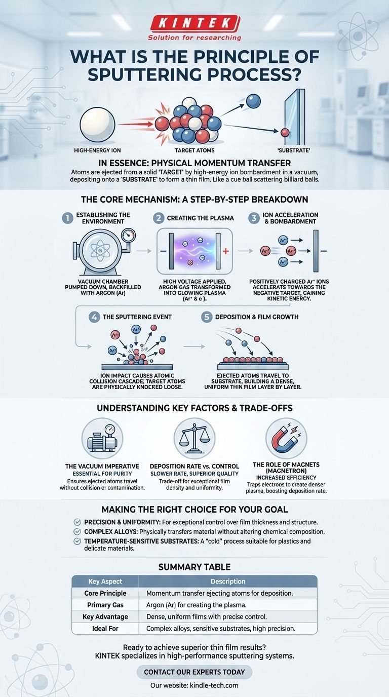
In essence, the principle of sputtering is a physical process where atoms are ejected from a solid material, known as a "target," by bombarding it with high-energy ions in a vacuum. These dislodged atoms then travel and deposit onto another surface, called a "substrate," to form an exceptionally thin and uniform film. The entire process relies on momentum transfer, much like a cue ball scattering billiard balls.
At its heart, sputtering is a physical momentum transfer process, not a chemical or thermal one. Think of it as a form of atomic-level sandblasting, where high-energy ions are used to precisely chip away at a source material, atom by atom, to build a new, ultra-thin film.
The Core Mechanism: A Step-by-Step Breakdown
To truly grasp the principle, it's best to visualize the process as a sequence of distinct events occurring within a controlled environment.
Step 1: Establishing the Environment
The process begins by placing both the target (the material you want to deposit) and the substrate (the object to be coated) inside a vacuum chamber.
This chamber is pumped down to a very low pressure and then backfilled with a small, controlled amount of an inert gas, most commonly Argon (Ar).
Step 2: Creating the Plasma
A high voltage is applied between the target and the substrate, with the target acting as the negative electrode (cathode).
This strong electric field energizes the inert Argon gas, stripping electrons from the Argon atoms and transforming the gas into a plasma—a glowing, energized state of matter consisting of positive ions (Ar+) and free electrons.
Step 3: Ion Acceleration and Bombardment
The positively charged Argon ions within the plasma are now strongly attracted and accelerated towards the negatively charged target.
They rush towards the target, gaining significant kinetic energy along the way.
Step 4: The Sputtering Event
Upon impact, the high-energy Argon ions collide with the surface of the target. This collision sets off a "collision cascade" within the target's atomic structure.
The momentum from the incoming ion is transferred to the target atoms. When atoms near the surface gain enough energy to overcome their atomic binding forces, they are physically knocked loose and ejected into the vacuum chamber. This ejection is the sputtering event.
Step 5: Deposition and Film Growth
The ejected target atoms travel through the vacuum chamber until they strike the substrate.
Upon arrival, they stick to the substrate, gradually building up, layer by layer, to form a dense and highly uniform thin film. Because this is a physical, atom-by-atom process, it allows for incredible control over the film's thickness and properties.
Understanding the Trade-offs and Key Factors
The elegance of the sputtering principle lies in its control, but this comes with inherent complexities and trade-offs that are critical to understand.
The Vacuum Imperative
A high vacuum is not optional; it is essential. It ensures that sputtered atoms can travel from the target to the substrate without colliding with unwanted air or gas molecules, which would contaminate the film. This requirement adds to the cost and complexity of the equipment.
Deposition Rate vs. Control
Compared to some other methods like thermal evaporation, basic sputtering can be a relatively slow process. This slower rate is the direct trade-off for the superior film quality, density, and uniformity it provides.
The Role of Magnets
To increase the slow deposition rate, a common enhancement called magnetron sputtering is used. Magnets are placed behind the target to trap electrons near its surface. These trapped electrons cause more efficient ionization of the Argon gas, creating a denser plasma that leads to a much higher rate of bombardment and, consequently, faster film growth.
Making the Right Choice for Your Goal
Understanding this principle allows you to determine when sputtering is the most effective method for your specific material engineering challenge.
- If your primary focus is precision and uniformity: Sputtering is ideal because the atom-by-atom deposition provides exceptional control over film thickness, density, and structure.
- If your primary focus is coating with complex materials or alloys: Sputtering excels because it physically transfers the target material without altering its chemical composition, ensuring the film matches the source.
- If your primary focus is coating temperature-sensitive substrates: Sputtering is a "cold" process compared to thermal evaporation, making it suitable for coating materials like plastics that cannot withstand high heat.
By grasping this atomic-level mechanism, you can better leverage its power to engineer materials with exacting specifications.
Summary Table:
| Key Aspect | Description |
|---|---|
| Core Principle | Momentum transfer from high-energy ions to a target material, ejecting atoms for deposition. |
| Primary Gas | Argon (Ar), used to create the plasma for ion bombardment. |
| Key Advantage | Produces dense, highly uniform thin films with precise control over composition. |
| Ideal For | Coating complex alloys, temperature-sensitive substrates, and applications requiring high precision. |
Ready to achieve superior thin film results?
KINTEK specializes in high-performance sputtering systems and consumables for your laboratory. Whether you are developing new materials, working with sensitive substrates, or require unparalleled film uniformity, our expertise and equipment are designed to meet your precise needs.
Contact our experts today to discuss how our solutions can enhance your research and development process.
Visual Guide
Related Products
- Three-dimensional electromagnetic sieving instrument
- Chemical Vapor Deposition CVD Equipment System Chamber Slide PECVD Tube Furnace with Liquid Gasifier PECVD Machine
- Customer Made Versatile CVD Tube Furnace Chemical Vapor Deposition Chamber System Equipment
- Twin Screw Extruder Plastic Granulation Machine
- HFCVD Machine System Equipment for Drawing Die Nano-Diamond Coating
People Also Ask
- What are the limitations of sieving? Understanding the Constraints of Particle Size Analysis
- How is sieving important? The Critical Role of Particle Size Analysis in Quality Control
- Why is sieving equipment essential for the classification of processed bio-activated carbon? Optimize Performance
- What are the precautions for sieving method? Ensure Accurate Particle Size Analysis
- What is sieving and how does it work? A Guide to Accurate Particle Size Analysis