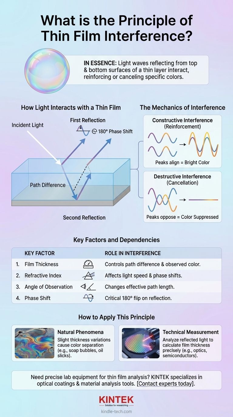
In essence, thin film interference is the phenomenon where light waves reflecting from the top and bottom surfaces of a very thin layer of material interact with each other. This interaction, or interference, either reinforces certain colors (wavelengths) or cancels them out, creating the vibrant colors seen in soap bubbles or oil slicks.
The core principle is that the thickness of the film dictates the path a light wave travels. This path difference determines whether the reflected waves are in-sync (constructive interference) or out-of-sync (destructive interference), which in turn controls which colors are reflected and which are suppressed.
How Light Interacts with a Thin Film
To understand the principle, we must trace the journey of light as it encounters a thin film, such as a layer of oil on water.
The First Reflection
When a light wave strikes the top surface of the film, a portion of it reflects back immediately. Another portion of the light passes through the film's top surface and continues traveling downward.
The Second Reflection
The light that entered the film travels through it until it reaches the bottom surface. At this boundary, it reflects again, traveling back up through the film and exiting out the top surface.
The Critical Path Difference
We now have two reflected light waves traveling in the same direction. However, the second wave traveled a longer distance—down and back up through the film. This extra distance is known as the path difference.
The Phase Shift on Reflection
A crucial event happens during reflection. When light reflects off a material with a higher refractive index (a denser medium), the wave is essentially "flipped," undergoing a 180-degree phase shift. This flip is critical for determining how the two waves will ultimately interact.
The Mechanics of Interference
The final visible effect is determined by how these two reflected waves, with their specific path difference and phase shifts, combine.
Constructive Interference (Reinforcement)
If the peaks and troughs of the two reflected waves align perfectly (they are "in phase"), they combine to create a stronger, brighter wave. This is constructive interference, and it makes that specific color (wavelength) appear bright and vibrant.
Destructive Interference (Cancellation)
If the peaks of one wave align with the troughs of the other (they are "out of phase"), they cancel each other out. This is destructive interference, which effectively removes that specific color from the light you see reflected.
Key Factors and Dependencies
The outcome of interference is not random; it is governed by a few precise physical properties.
The Role of Film Thickness
Film thickness is the most critical factor. It directly controls the path difference between the two reflected waves. A change in thickness, even by a few nanometers, will change which wavelengths interfere constructively or destructively, thus changing the observed color.
The Impact of Refractive Index
The refractive index of the film material (and the materials above and below it) is also essential. It determines the speed of light within the film, which affects the path difference, and it dictates whether a phase shift occurs upon reflection at each surface.
The Angle of Observation
The angle at which you view the film also changes the path length of the light traveling within it. This is why the colors on an oil slick or soap bubble appear to shift and swirl as you change your viewing position.
How to Apply This Principle
Understanding thin film interference is valuable for both interpreting natural phenomena and for precision engineering.
- If your primary focus is on natural phenomena: The key is that slight variations in a film's thickness cause white light to separate into its constituent colors by selectively reinforcing some and canceling others.
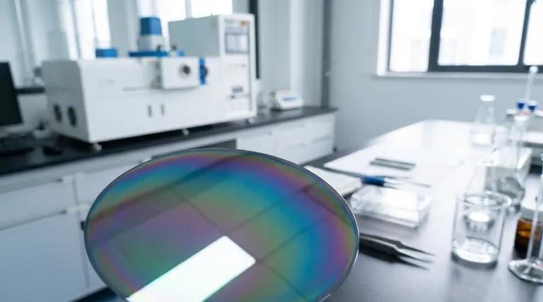
- If your primary focus is on technical measurement: The key is that by analyzing the specific pattern of reflected light, you can calculate a film's thickness with incredible precision, a vital technique in manufacturing semiconductors and optical coatings.
This interplay between light, thickness, and material properties is a fundamental principle that makes the invisible world of the nanoscale visible to the naked eye.
Summary Table:
| Key Factor | Role in Interference |
|---|---|
| Film Thickness | Determines the path difference, controlling which colors are reinforced or canceled. |
| Refractive Index | Affects light speed and phase shifts upon reflection at each surface. |
| Angle of Observation | Changes the effective path length, causing colors to shift with viewing angle. |
| Phase Shift | A 180-degree 'flip' upon reflection from a denser medium is critical for interference. |
Need to measure or apply thin film principles in your lab? KINTEK specializes in the precise lab equipment and consumables you need to work with optical coatings, semiconductors, and material analysis. Our expertise ensures you have the right tools to achieve accurate results. Contact our experts today to discuss your specific application!
Visual Guide