The primary advantages of sputtering are its exceptional versatility in handling nearly any material, the superior quality and adhesion of the films it produces, and the high degree of process control it offers. Unlike other methods, sputtering uses high-energy ion bombardment to physically eject atoms from a source target, resulting in dense, pure, and strongly bonded thin films on a substrate with excellent thickness uniformity, even over large areas.
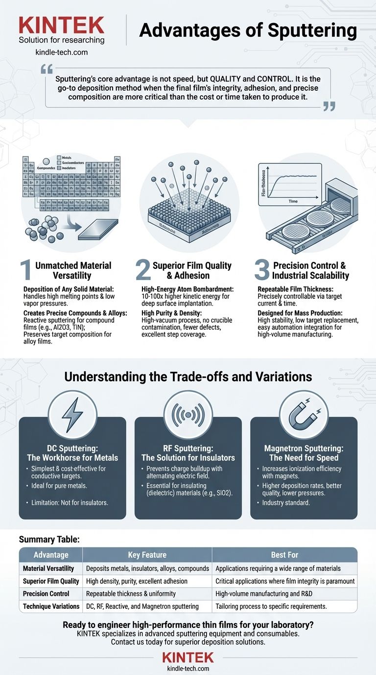
Sputtering's core advantage is not speed, but quality and control. It is the go-to deposition method when the final film's integrity, adhesion, and precise composition are more critical than the cost or time taken to produce it.
Unmatched Material Versatility
One of sputtering's most significant strengths is its ability to deposit films from an incredibly wide range of source materials. This flexibility makes it suitable for countless applications in semiconductors, optics, and materials science.
Deposition of Any Solid Material
Because sputtering is a physical momentum-transfer process rather than a chemical or thermal one, it can be used on virtually any substance. This includes elements and compounds with extremely high melting points and low vapor pressures that are difficult or impossible to deposit using thermal evaporation.
It can effectively deposit metals, semiconductors, insulators, and complex mixtures.
Creating Precise Compounds and Alloys
Sputtering excels at creating films with specific chemical compositions. Reactive sputtering, where a reactive gas like oxygen or nitrogen is introduced, is one of the easiest methods to create compound films like aluminum oxide (Al2O3) or titanium nitride (TiN) with precise stoichiometry.
Furthermore, sputtering can deposit alloy films while preserving the original composition of the target material, a significant advantage for creating materials with specific electronic or mechanical properties.
Superior Film Quality and Adhesion
Sputtered films are renowned for their high quality, which stems directly from the physics of the deposition process. The resulting films are dense, pure, and exceptionally well-bonded to the substrate.
The Role of High-Energy Atoms
Sputtered atoms are ejected from the target with significantly higher kinetic energy (10-100 times more) than evaporated atoms. This high energy allows them to physically implant into the substrate's surface, creating a strong diffusion layer.
This results in excellent adhesion that is far superior to many other deposition techniques.
High Purity and Film Density
The sputtering process occurs in a high-vacuum environment and does not involve melting the source material, which eliminates contamination from a crucible or heating element.
This leads to films with high purity, high density, and fewer pinholes or other defects. The process also provides excellent step coverage, meaning it can uniformly coat substrates with complex, non-flat topologies.
Precision Control and Industrial Scalability
Sputtering is a highly controllable and reproducible process, making it ideal for high-volume manufacturing where consistency is paramount.
Repeatable Film Thickness and Uniformity
Film thickness is directly proportional to the target current and deposition time, allowing for precise and repeatable control. Sputtering systems are engineered to produce highly uniform films across large areas, a critical requirement for manufacturing wafers and large optical components.
Designed for Mass Production
The process is highly stable and reliable. Key advantages for industrial settings include a low target replacement frequency and easy integration into automated, single-wafer processing lines, making sputtering a cornerstone of modern manufacturing.
Understanding the Trade-offs and Variations
While sputtering is broadly advantageous, the specific technique used depends on the target material and desired outcome. Each variation offers a different balance of cost, speed, and capability.
DC Sputtering: The Workhorse for Metals
Direct Current (DC) sputtering is the simplest and most cost-effective method. It is highly effective for depositing electrically conductive targets like pure metals. Its key advantages are ease of control and low equipment cost.
Its major limitation is that it cannot be used on insulating materials, as positive charge builds up on the target surface, halting the process.
RF Sputtering: The Solution for Insulators
Radio Frequency (RF) sputtering uses an alternating electric field to prevent charge buildup on the target. This makes it the essential technique for depositing insulating (dielectric) materials like ceramics and oxides (e.g., SiO2).
While more complex and expensive than DC sputtering, it dramatically expands the range of materials that can be deposited.
Magnetron Sputtering: The Need for Speed
Magnetron sputtering incorporates strong magnets behind the target. These magnets trap electrons near the target surface, significantly increasing the ionization efficiency of the sputtering gas.
This results in a much denser plasma, leading to higher deposition rates, better surface quality, and lower operating pressures. Today, most modern sputtering systems are magnetron-based due to these performance gains.
Making the Right Choice for Your Goal
Selecting the right sputtering technique is critical to achieving your desired outcome efficiently and cost-effectively.
- If your primary focus is depositing pure metals or conductive materials at the lowest cost: DC sputtering is the most straightforward and economical choice.
- If your primary focus is depositing insulating materials like ceramics or oxides: RF sputtering is the necessary and correct technology for the job.
- If your primary focus is creating high-purity compound films with exact stoichiometry: Reactive sputtering is the ideal method.
- If your primary focus is high-volume manufacturing requiring maximum speed and efficiency: Magnetron sputtering is the industry standard for achieving high deposition rates and superior film quality.
Ultimately, sputtering provides an unparalleled toolkit for engineering high-quality, high-performance thin films for nearly any application.
Summary Table:
| Advantage | Key Feature | Best For |
|---|---|---|
| Material Versatility | Deposits metals, insulators, alloys, and compounds | Applications requiring a wide range of materials |
| Superior Film Quality | High density, purity, and excellent adhesion | Critical applications where film integrity is paramount |
| Precision Control | Repeatable thickness and uniformity over large areas | High-volume manufacturing and R&D |
| Technique Variations | DC, RF, Reactive, and Magnetron sputtering | Tailoring the process to specific material and speed requirements |
Ready to engineer high-performance thin films for your laboratory? KINTEK specializes in advanced sputtering equipment and consumables, providing the precision and reliability your lab needs for semiconductor, optics, and materials science applications. Contact us today to discuss how our solutions can enhance your deposition processes and deliver superior results.
Visual Guide
Related Products
- Spark Plasma Sintering Furnace SPS Furnace
- Vacuum Induction Melting Spinning System Arc Melting Furnace
- Chemical Vapor Deposition CVD Equipment System Chamber Slide PECVD Tube Furnace with Liquid Gasifier PECVD Machine
- Customer Made Versatile CVD Tube Furnace Chemical Vapor Deposition Chamber System Equipment
- Vacuum Cold Mounting Machine for Sample Preparation
People Also Ask
- What are the fundamentals of spark plasma sintering process? Unlock Rapid, High-Performance Material Consolidation
- What technical advantages does a Spark Plasma Sintering (SPS) furnace offer for LZP ceramics? Enhance Ionic Conductivity
- What is the theory of spark plasma sintering? A Guide to Rapid, Low-Temperature Densification
- Why are Spark Plasma Sintering (SPS) furnaces or hot presses utilized in the preparation of Li3PS4 solid electrolytes?
- What are the advantages of CAMI/SPS for W-Cu composite preparation? Reduce cycles from hours to seconds.


