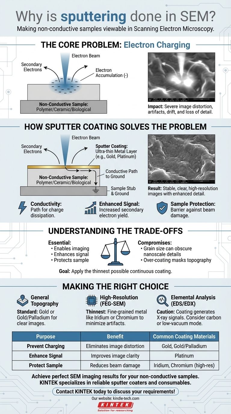
In Scanning Electron Microscopy (SEM), sputtering is performed to make non-conductive samples viewable. The process applies an ultra-thin, electrically conductive layer—typically of a metal like gold or platinum—onto a specimen. This coating prevents severe image distortion and allows for the capture of clear, high-resolution images that would otherwise be impossible to obtain.
The core purpose of sputter coating is to solve the problem of "electron charging." When an electron beam hits a non-conductive surface, electrons accumulate, creating a static charge that deflects the beam and ruins the image. Sputtering creates a conductive pathway for these electrons to escape to ground, stabilizing the sample for analysis.
The Core Problem: Electron Charging
Before a sample is coated, it is essential to understand why the step is necessary. The issue originates from the fundamental way an SEM works: by bombarding a specimen with a focused beam of electrons.
What is "Charging"?
An SEM image is formed by detecting signals—primarily secondary electrons—that are ejected from the sample's surface when hit by the primary electron beam.
On a conductive sample, any excess negative charge from the beam is immediately conducted away to ground.
On a non-conductive sample (like a polymer, ceramic, or biological tissue), these electrons have nowhere to go. They accumulate on the surface, creating a localized negative charge.
The Impact of Charging on Image Quality
This accumulated charge, known as "charging," is highly detrimental to SEM imaging. It can deflect the incoming electron beam and interfere with the trajectory of the outgoing secondary electrons.
The result is a range of severe image artifacts, including:
- Unnaturally bright or glowing areas
- Distorted or warped features
- Image drift or shifting during a scan
- A complete loss of detail and resolution
In essence, charging makes it impossible to acquire a stable, accurate, or high-quality image of the sample's true surface.
How Sputter Coating Solves the Problem
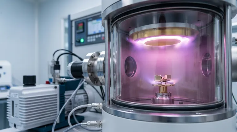
Sputter coating is a sample preparation technique that deposits a metallic film, typically just 2-20 nanometers thick, over the entire surface of the specimen. This thin layer solves the charging problem in several key ways.
Creating a Conductive Path to Ground
The most critical function of the coating is providing electrical conductivity. The metal layer creates a continuous path from the point of beam interaction to the sample holder (stub) and then to the microscope's electrical ground.
This path allows the excess electrons from the beam to dissipate instantly, preventing any charge from building up on the surface.
Enhancing the Signal for Clearer Images
Most sputter coating materials, like gold and platinum, are excellent emitters of secondary electrons. They release more of these signal-carrying electrons per incoming primary electron than typical non-conductive materials do.
This increases the overall signal detected by the microscope, significantly improving the signal-to-noise ratio. The resulting image is sharper, clearer, and richer in topographical detail.
Protecting the Specimen from Beam Damage
The electron beam carries a significant amount of energy, which can damage or "burn" delicate samples like polymers or biological specimens.
The metallic coating acts as a protective barrier, absorbing and dispersing much of this energy. It also improves thermal conduction, helping to draw heat away from the sample and further reduce the risk of thermal damage.
Understanding the Trade-offs
While essential, sputter coating is not without its compromises. An operator must understand the trade-offs to ensure the coating itself does not interfere with the analysis.
The Coating Can Obscure Fine Details
The sputtered metal is not a perfectly smooth film; it is composed of tiny grains. The size of these grains can obscure the finest nanoscale features on a sample's surface.
For high-resolution work, metals with smaller grain sizes (like iridium or chromium) are preferred over gold, which has a larger grain structure.
The Risk of Over-coating
Applying a coating that is too thick is a common mistake. An overly thick layer will mask the sample's true topography, and the image you capture will be of the coating's surface, not the specimen's.
The goal is always to apply the thinnest possible continuous coating that effectively prevents charging.
Making the Right Choice for Your Goal
Sputtering is a foundational technique, but its application should be tailored to your analytical objective.
- If your primary focus is general topographical imaging of a non-conductor: Sputter coating with gold or gold/palladium is the standard, most effective method to get a clear image.
- If your primary focus is very high-resolution imaging (FEG-SEM): Use the thinnest possible coating of a fine-grained metal like iridium or chromium to minimize artifacts and preserve nanoscale details.
- If your primary focus is elemental analysis (EDS/EDX): Remember the coating metal will generate strong X-ray signals. If this interferes with your analysis, consider using a carbon coater or operating the SEM in a low-vacuum mode without any coating.
Ultimately, sputter coating is the key that unlocks high-quality SEM imaging for the vast world of non-conductive materials.
Summary Table:
| Purpose | Benefit | Common Coating Materials |
|---|---|---|
| Prevent Charging | Eliminates image distortion and artifacts | Gold, Gold/Palladium |
| Enhance Signal | Improves image clarity and detail | Platinum |
| Protect Sample | Reduces beam damage to delicate specimens | Iridium, Chromium (for high-res) |
Achieve perfect SEM imaging results for your non-conductive samples.
Sputter coating is essential for clear, stable, and high-resolution images. KINTEK specializes in providing reliable sputter coaters and consumables tailored to your specific laboratory needs—whether for biological samples, polymers, or advanced materials research.
Let our experts help you select the ideal coating solution for your application. Contact KINTEK today to discuss your requirements and enhance your SEM analysis!
Visual Guide
Related Products
People Also Ask
- What is the specific function of the metal filament in HF-CVD? Key Roles in Diamond Growth
- What are the disadvantages and challenges of the HFCVD method? Overcome Growth Limits and Filament Issues
- Why is Chemical Vapor Deposition (CVD) equipment uniquely suited for constructing hierarchical superhydrophobic structures?
- What is the full form of HFCVD? A Guide to Hot Filament Chemical Vapor Deposition
- How expensive is chemical vapor deposition? Understanding the True Cost of High-Performance Coating
