Lab Materials
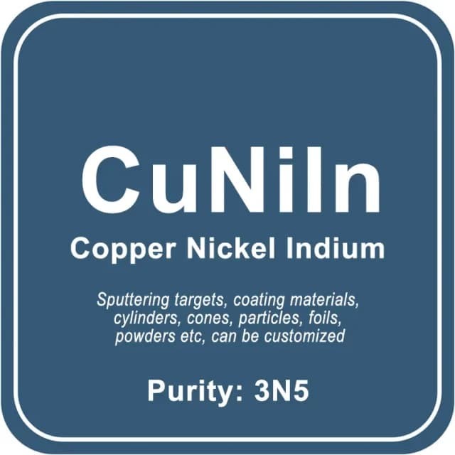
Copper Nickel Indium Alloy (CuNiIn) Sputtering Target / Powder / Wire / Block / Granule
Item Number : LM-CuNiIn
Price varies based on specs and customizations
- Chemical Formula
- CuNiIn
- Purity
- 3N5
- Commonly Used Ratio
- Cu:Ni:ln=59:36:5 wt%
- Shape
- discs / wire / block / powder / plates / column targets / step target / custom-made

Shipping:
Contact us to get shipping details Enjoy On-time Dispatch Guarantee.
We offer Copper Nickel Indium Alloy (CuNiIn) materials at reasonable prices for laboratory use. Our expertise lies in producing and tailoring CuNiIn materials of different purities, shapes, and sizes to meet your unique requirements.
We provide a wide range of specifications and sizes for various products, including sputtering targets (circular, square, tubular, and irregular shapes), coating materials, cylinders, cones, particles, foils, powders, 3D printing powders, nanometer powders, wire rods, ingots, and blocks, among others.
Details


About Copper Nickel Indium Alloy (CuNiIn)
Copper Nickel Indium Alloy is often used as neutron-absorbing materials in atomic reactors, as well as in microwave technology and phosphors for color TVs
Ingredient Quality Control
- Raw material composition analysis
- Through the use of equipment such as ICP and GDMS, the content of metal impurities is detected and analyzed to ensure that it meets the purity standard;
Non-metallic impurities are detected by equipment such as carbon and sulfur analyzers, nitrogen and oxygen analyzers. - Metallographic flaw detection analysis
- The target material is inspected using flaw detection equipment to ensure that there are no defects or shrinkage holes inside the product;
Through metallographic testing, the internal grain structure of the target material is analyzed to ensure that the grains are fine and dense. - Appearance and dimension inspection
- Product dimensions are measured using micrometers and precision calipers to ensure compliance with drawings;
The surface finish and cleanliness of the product are measured using a surface cleanliness meter.
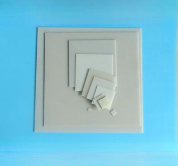
Conventional Sputtering Target Sizes
- Preparation process
- hot isostatic pressing, vacuum melting, etc.
- Sputtering target shape
- plane sputtering target, multi-arc sputtering target, step sputtering target, special-shaped sputtering target
- Round sputtering target size
- Diameter: 25.4mm / 50mm / 50.8mm / 60mm / 76.2mm / 80mm / 100mm / 101.6mm / 152.4mm
Thickness: 3mm / 4mm / 5mm / 6mm / 6.35mm
Size can be customized. - Square sputtering target size
- 50×50×3mm / 100×100×4mm / 300×300×5mm, size can be customized
Available Metal Forms
Metal Forms Details
We manufacture almost all the metals listed on the periodic table in a wide range of forms and purities, as well as standard sizes and dimensions. We can also produce custom-made products to meet specific customer requirements, such as size, shape, surface area, composition, and more. The following list provides a sample of the forms we offer, but it is not exhaustive. If you need laboratory consumables, please contact us directly to request a quote.
- Flat/Planar Forms: Board, Film, Foil, Microfoil, Microleaf, Paper, Plate, Ribbon, Sheet, Strip, Tape, Wafer
- Preformed Shapes: Anodes, Balls, Bands, Bars, Boats, Bolts, Briquettes, Cathodes, Circles, Coils, Crucibles, Crystals, Cubes, Cups, Cylinders, Discs, Electrodes, Fibers, Filaments, Flanges, Grids, Lenses, Mandrels, Nuts, Parts, Prisms, Pucks, Rings, Rods, Shapes, Shields, Sleeves, Springs, Squares, Sputtering Targets, Sticks, Tubes, Washers, Windows, Wires
- Microsizes: Beads, Bits, Capsules, Chips, Coins, Dust, Flakes, Grains, Granules, Micropowder, Needles, Particles, Pebbles, Pellets, Pins, Pills, Powder, Shavings, Shot, Slugs, Spheres, Tablets
- Macrosizes: Billets, Chunks, Cuttings, Fragments, Ingots, Lumps, Nuggets, Pieces, Punchings, Rocks, Scraps, Segments, Turnings
- Porous and Semi-Porous: Fabric, Foam, Gauze, Honeycomb, Mesh, Sponge, Wool
- Nanoscale: Nanoparticles, Nanopowders, Nanofoils, Nanotubes, Nanorods, Nanoprisms
- Others: Concentrate, Ink, Paste, Precipitate, Residue, Samples, Specimens
KinTek specializes in the manufacturing of high-purity and ultra-high-purity materials with a purity range of 99.999% (5N), 99.9999% (6N), 99.99995% (6N5), and in some cases, up to 99.99999% (7N). Our materials are available in specific grades, including UP/UHP, semiconductor, electronic, deposition, fiber optic, and MBE grades. Our high-purity metals, oxides, and compounds are specifically crafted to meet the rigorous demands of high-technology applications and are ideal for use as dopants and precursor materials for thin film deposition, crystal growth of semiconductors, and synthesis of nanomaterials. These materials find use in advanced microelectronics, solar cells, fuel cells, optical materials, and other cutting-edge applications.
Packaging
We use vacuum packaging for our high-purity materials, and each material has specific packaging tailored to its unique characteristics. For instance, our Hf sputter target is externally tagged and labeled to facilitate efficient identification and quality control. We take great care to prevent any damage that could occur during storage or transportation.
4.7
out of
5
KINTEK's CuNiIn materials are truly remarkable. Their high purity and uniformity ensure consistent and reliable performance in our sputtering processes.
4.8
out of
5
The Copper Nickel Indium Alloy targets we received from KINTEK are of exceptional quality. They have significantly improved the efficiency of our sputtering system.
4.9
out of
5
We have been using KINTEK's CuNiIn sputtering targets for over a year now and have been very impressed with their durability and performance. They have consistently met our high standards.
4.7
out of
5
KINTEK's CuNiIn materials have enabled us to achieve remarkable results in our research. Their purity and consistency have been instrumental in our success.
4.8
out of
5
The technical support we received from KINTEK was outstanding. They went above and beyond to help us optimize our sputtering process and achieve the desired results.
4.9
out of
5
The CuNiIn powders we purchased from KINTEK were of exceptional quality and purity. They have greatly contributed to the success of our 3D printing experiments.
4.7
out of
5
KINTEK's CuNiIn sputtering targets have significantly reduced downtime in our production process. Their durability and reliability have been a game-changer for us.
4.8
out of
5
The Copper Nickel Indium Alloy wires we received from KINTEK were precisely manufactured and met our exact specifications. They have performed flawlessly in our application.
4.9
out of
5
We were thoroughly impressed with the fast delivery of our CuNiIn sputtering targets from KINTEK. Their commitment to timely service is truly commendable.
4.7
out of
5
KINTEK's CuNiIn materials have consistently exceeded our expectations. Their high quality and reliability have made them our go-to supplier for sputtering targets.
4.8
out of
5
The Copper Nickel Indium Alloy blocks we procured from KINTEK were of exceptional quality and met our stringent requirements. They have been instrumental in our research endeavors.
4.9
out of
5
We have been using KINTEK's CuNiIn sputtering targets for several years now and have never encountered any issues. Their consistency and reliability are truly remarkable.
4.7
out of
5
KINTEK's CuNiIn materials have enabled us to push the boundaries of our research. Their exceptional purity and uniformity have been crucial to our success.
4.8
out of
5
The technical expertise provided by KINTEK's team was invaluable. They helped us optimize our sputtering process and achieve the desired results efficiently.
4.9
out of
5
The CuNiIn granules we received from KINTEK were of exceptional quality and purity. They have significantly improved the performance of our sputtering system.
4.7
out of
5
KINTEK's CuNiIn sputtering targets have enabled us to achieve remarkable results in our thin-film deposition experiments. Their high purity and uniformity have been key factors in our success.
4.8
out of
5
The Copper Nickel Indium Alloy powders we procured from KINTEK were of exceptional quality and purity. They have greatly contributed to the success of our research projects.
4.9
out of
5
We have been using KINTEK's CuNiIn materials for several years now and have been consistently impressed with their quality and performance. They have become an integral part of our research and development efforts.
REQUEST A QUOTE
Our professional team will reply to you within one business day. Please feel free to contact us!
Related Products
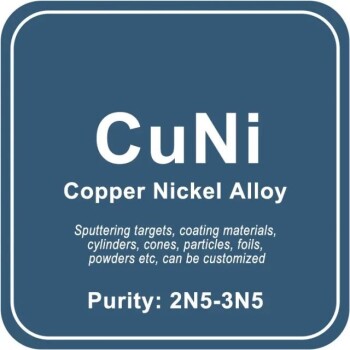
Copper Nickel Alloy (CuNi) Sputtering Target / Powder / Wire / Block / Granule
Get high-quality Copper Nickel Alloy (CuNi) materials at affordable prices for your laboratory needs. Our customized offerings include sputtering targets, coatings, powders, and more. Order now!
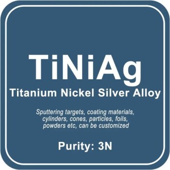
Titanium Nickel Silver Alloy (TiNiAg) Sputtering Target / Powder / Wire / Block / Granule
Looking for customizable TiNiAg materials? We offer a wide range of sizes and purities at competitive prices, including sputtering targets, coating materials, powders, and more. Contact us today!
Nickel Niobium Alloy (NiNb) Sputtering Target / Powder / Wire / Block / Granule
Find high-quality Nickel Niobium Alloy (NiNb) materials for your laboratory needs. We offer tailored purities, shapes, and sizes, plus sputtering targets, coatings, powders, and more. Explore our range now!
Iron Nickel Alloy (FeNi) Sputtering Target / Powder / Wire / Block / Granule
Discover affordable Iron Nickel Alloy materials tailored to your lab's needs. Our FeNi products come in various sizes and shapes, from sputtering targets to powders and ingots. Order now!
Aluminum Copper Alloy (AlCu) Sputtering Target / Powder / Wire / Block / Granule
Get high-quality Aluminum Copper Alloy (AlCu) materials for your laboratory needs at affordable prices. Customized purities, shapes, and sizes available. Shop sputtering targets, coating materials, powders, and more.
Nickel Aluminum Alloy (NiAl) Sputtering Target / Powder / Wire / Block / Granule
Looking for high-quality Nickel Aluminum Alloy materials for your lab? Our experts produce and customize NiAl materials to suit your specific needs. Find a wide range of sizes and specifications for sputtering targets, coating materials, and more at affordable prices.
Manganese Cobalt Nickel alloy (MnCoNi) Sputtering Target / Powder / Wire / Block / Granule
Get top-quality Manganese Cobalt Nickel alloy materials for your laboratory needs at affordable prices. Our customized products come in various sizes and shapes, including sputtering targets, coating materials, powders, and more.
Chromium Nickel Alloy (CrNi) Sputtering Target / Powder / Wire / Block / Granule
Looking for high-quality Chromium Nickel Alloy (CrNi) materials for your lab? Look no further than our expertly crafted and tailored options. Explore our wide range of sizes and specifications, including sputtering targets, coatings, powders, and more. Shop now!
Copper Zirconium Alloy (CuZr) Sputtering Target / Powder / Wire / Block / Granule
Discover our range of Copper Zirconium Alloy materials at affordable prices, tailored to your unique requirements. Browse our selection of sputtering targets, coatings, powders, and more.
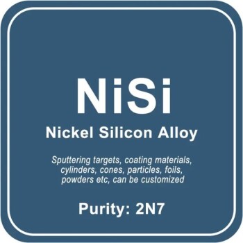
Nickel Silicon Alloy (NiSi) Sputtering Target / Powder / Wire / Block / Granule
Looking for Nickel Silicon Alloy materials for your lab? Our expertly produced and tailored materials come in various shapes and sizes to suit your unique needs. Get sputtering targets, coating materials, powders, and more at reasonable prices.
Nickel Chromium Alloy (NiCr) Sputtering Target / Powder / Wire / Block / Granule
Get high-quality Nickel Chromium Alloy (NiCr) materials for your lab needs at affordable prices. Choose from a wide range of shapes and sizes, including sputtering targets, coatings, powders, and more. Tailored to suit your unique requirements.
High Purity Nickel (Ni) Sputtering Target / Powder / Wire / Block / Granule
Looking for high-quality Nickel (Ni) materials for laboratory use? Look no further than our customizable selection! With competitive prices and a range of sizes and shapes to choose from, we have everything you need to meet your unique requirements.

Tin Bismuth Silver Alloy (SnBiAg) Sputtering Target / Powder / Wire / Block / Granule
Discover our high-quality Tin Bismuth Silver Alloy materials at reasonable prices. We offer a wide range of customized shapes and sizes for your laboratory needs. Shop sputtering targets, coatings, powders, and more today.
Aluminum Nitride (AlN) Ceramic Sheet
Aluminum nitride (AlN) has the characteristics of good compatibility with silicon. It is not only used as a sintering aid or reinforcing phase for structural ceramics, but its performance far exceeds that of alumina.