Lab Materials
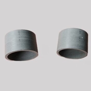
High Purity Nickel (Ni) Sputtering Target / Powder / Wire / Block / Granule
Item Number : LM-NI
Price varies based on specs and customizations
- Chemical Formula
- Ni
- Purity
- 3N-5N
- Shape
- discs / wire / block / powder / plates / column targets / step target / custom-made

Shipping:
Contact us to get shipping details Enjoy On-time Dispatch Guarantee.
We are pleased to offer Nickel (Ni) materials for laboratory use at competitive prices. Our specialty lies in manufacturing and customizing Nickel (Ni) materials of varying purities, shapes, and sizes to meet your specific needs.
Our extensive selection includes a variety of specifications and sizes for sputtering targets (circular, square, tubular, irregular), coating materials, cylinders, cones, particles, foils, powders, 3D printing powders, nanometer powders, wire rods, ingots, blocks, and more.
Details


About Nickel (Ni)
Nickel is a widely used element in alloying with iron, chromium, molybdenum, and tungsten to produce stainless steel and other corrosion-resistant alloys. This is due to its unique properties, such as its ability to resist corrosion and maintain strength at high temperatures.
In addition to its use in alloys, nickel is also commonly used in electronics applications due to its high electrical conductivity. For example, it is used in nickel hydride batteries and ceramic anode formulations for oxygen generation and solid oxide fuel cells.
Nickel also has uses in the art world as a pigment. When added to glass and ceramic glazes, it creates a bright green color that is highly desired.
When it comes to sourcing nickel for scientific purposes, it is available in various forms such as metal, pellets, rod, wire, granules, nanoparticles, and nanopowders. It is also available in different compounds with purities ranging from 99% to 99.999% (ACS grade to ultra-high purity).
For applications requiring nickel oxides, they are available in powder and dense pellet form for uses such as optical coating and thin film applications. However, it is important to note that oxides tend to be insoluble. Nickel fluorides are another insoluble form used in metallurgy, chemical and physical vapor deposition, and some optical coatings. Soluble forms of nickel are also available, such as chlorides, nitrates, and acetates, which can be manufactured as solutions at specified stoichiometries.
Ingredient Quality Control
- Raw material composition analysis
- Through the use of equipment such as ICP and GDMS, the content of metal impurities is detected and analyzed to ensure that it meets the purity standard;
Non-metallic impurities are detected by equipment such as carbon and sulfur analyzers, nitrogen and oxygen analyzers. - Metallographic flaw detection analysis
- The target material is inspected using flaw detection equipment to ensure that there are no defects or shrinkage holes inside the product;
Through metallographic testing, the internal grain structure of the target material is analyzed to ensure that the grains are fine and dense. - Appearance and dimension inspection
- Product dimensions are measured using micrometers and precision calipers to ensure compliance with drawings;
The surface finish and cleanliness of the product are measured using a surface cleanliness meter.
Conventional Sputtering Target Sizes
- Preparation process
- hot isostatic pressing, vacuum melting, etc.
- Sputtering target shape
- plane sputtering target, multi-arc sputtering target, step sputtering target, special-shaped sputtering target
- Round sputtering target size
- Diameter: 25.4mm / 50mm / 50.8mm / 60mm / 76.2mm / 80mm / 100mm / 101.6mm / 152.4mm
Thickness: 3mm / 4mm / 5mm / 6mm / 6.35mm
Size can be customized. - Square sputtering target size
- 50×50×3mm / 100×100×4mm / 300×300×5mm, size can be customized
Available Metal Forms
Metal Forms Details
We manufacture almost all the metals listed on the periodic table in a wide range of forms and purities, as well as standard sizes and dimensions. We can also produce custom-made products to meet specific customer requirements, such as size, shape, surface area, composition, and more. The following list provides a sample of the forms we offer, but it is not exhaustive. If you need laboratory consumables, please contact us directly to request a quote.
- Flat/Planar Forms: Board, Film, Foil, Microfoil, Microleaf, Paper, Plate, Ribbon, Sheet, Strip, Tape, Wafer
- Preformed Shapes: Anodes, Balls, Bands, Bars, Boats, Bolts, Briquettes, Cathodes, Circles, Coils, Crucibles, Crystals, Cubes, Cups, Cylinders, Discs, Electrodes, Fibers, Filaments, Flanges, Grids, Lenses, Mandrels, Nuts, Parts, Prisms, Pucks, Rings, Rods, Shapes, Shields, Sleeves, Springs, Squares, Sputtering Targets, Sticks, Tubes, Washers, Windows, Wires
- Microsizes: Beads, Bits, Capsules, Chips, Coins, Dust, Flakes, Grains, Granules, Micropowder, Needles, Particles, Pebbles, Pellets, Pins, Pills, Powder, Shavings, Shot, Slugs, Spheres, Tablets
- Macrosizes: Billets, Chunks, Cuttings, Fragments, Ingots, Lumps, Nuggets, Pieces, Punchings, Rocks, Scraps, Segments, Turnings
- Porous and Semi-Porous: Fabric, Foam, Gauze, Honeycomb, Mesh, Sponge, Wool
- Nanoscale: Nanoparticles, Nanopowders, Nanofoils, Nanotubes, Nanorods, Nanoprisms
- Others: Concentrate, Ink, Paste, Precipitate, Residue, Samples, Specimens
KinTek specializes in the manufacturing of high-purity and ultra-high-purity materials with a purity range of 99.999% (5N), 99.9999% (6N), 99.99995% (6N5), and in some cases, up to 99.99999% (7N). Our materials are available in specific grades, including UP/UHP, semiconductor, electronic, deposition, fiber optic, and MBE grades. Our high-purity metals, oxides, and compounds are specifically crafted to meet the rigorous demands of high-technology applications and are ideal for use as dopants and precursor materials for thin film deposition, crystal growth of semiconductors, and synthesis of nanomaterials. These materials find use in advanced microelectronics, solar cells, fuel cells, optical materials, and other cutting-edge applications.
Packaging
We use vacuum packaging for our high-purity materials, and each material has specific packaging tailored to its unique characteristics. For instance, our Hf sputter target is externally tagged and labeled to facilitate efficient identification and quality control. We take great care to prevent any damage that could occur during storage or transportation.
FAQ
What Are High Purity Metals?
What Are High Purity Metals Used For?
What Are The Benefits Of Using High-purity Metals?
Which Industries Commonly Use High-purity Metals?
4.8
out of
5
I was so impressed with the quality of the nickel sputtering target I received from KINTEK SOLUTION. It is clear that they use high-quality materials and take great care in manufacturing their products.
4.7
out of
5
The nickel sputtering target I ordered from KINTEK SOLUTION arrived quickly and was exactly as described. I am very happy with the product and the service I received.
4.9
out of
5
I have been using KINTEK SOLUTION's nickel sputtering targets for years and have always been impressed with their quality and consistency. I highly recommend their products to anyone looking for high-quality sputtering targets.
4.6
out of
5
I was very happy with the nickel sputtering target I received from KINTEK SOLUTION. It was well-packaged and arrived in perfect condition. I would definitely order from them again.
4.8
out of
5
I am very satisfied with the nickel sputtering target I purchased from KINTEK SOLUTION. It is made of high-quality materials and has performed flawlessly in my experiments.
4.7
out of
5
I was very impressed with the quality of the nickel sputtering target I received from KINTEK SOLUTION. It is clear that they take great pride in their work.
4.9
out of
5
I have been using KINTEK SOLUTION's nickel sputtering targets for over a year now and have never had any problems with them. They are very reliable and produce high-quality results.
4.6
out of
5
I was very happy with the nickel sputtering target I received from KINTEK SOLUTION. It was exactly what I needed and arrived quickly.
4.8
out of
5
I am very impressed with the quality of the nickel sputtering target I received from KINTEK SOLUTION. It is clear that they use high-quality materials and take great care in manufacturing their products.
4.7
out of
5
The nickel sputtering target I ordered from KINTEK SOLUTION arrived quickly and was exactly as described. I am very happy with the product and the service I received.
4.9
out of
5
I have been using KINTEK SOLUTION's nickel sputtering targets for years and have always been impressed with their quality and consistency. I highly recommend their products to anyone looking for high-quality sputtering targets.
REQUEST A QUOTE
Our professional team will reply to you within one business day. Please feel free to contact us!
Related Products
Nickel Niobium Alloy (NiNb) Sputtering Target / Powder / Wire / Block / Granule
Find high-quality Nickel Niobium Alloy (NiNb) materials for your laboratory needs. We offer tailored purities, shapes, and sizes, plus sputtering targets, coatings, powders, and more. Explore our range now!
High Purity Nickel Oxide (Ni2O3) Sputtering Target / Powder / Wire / Block / Granule
Find high-quality Nickel Oxide materials for your laboratory needs at affordable prices. Our tailored solutions fit your specific requirements. Discover a range of shapes, sizes, and specifications for sputtering targets, coatings, powders, and more.
Nickel Silicon Alloy (NiSi) Sputtering Target / Powder / Wire / Block / Granule
Looking for Nickel Silicon Alloy materials for your lab? Our expertly produced and tailored materials come in various shapes and sizes to suit your unique needs. Get sputtering targets, coating materials, powders, and more at reasonable prices.
Nickel Chromium Alloy (NiCr) Sputtering Target / Powder / Wire / Block / Granule
Get high-quality Nickel Chromium Alloy (NiCr) materials for your lab needs at affordable prices. Choose from a wide range of shapes and sizes, including sputtering targets, coatings, powders, and more. Tailored to suit your unique requirements.
Copper Nickel Alloy (CuNi) Sputtering Target / Powder / Wire / Block / Granule
Get high-quality Copper Nickel Alloy (CuNi) materials at affordable prices for your laboratory needs. Our customized offerings include sputtering targets, coatings, powders, and more. Order now!

High Purity Niobium (Nb) Sputtering Target / Powder / Wire / Block / Granule
Looking for customized Niobium materials for laboratory use? Our experts offer tailored solutions with different purities, shapes, and sizes at reasonable prices. Discover our wide range of Niobium products.
Nickel foam is a high-tech deep-processing, and the metal nickel is made into a foam sponge, which has a three-dimensional full-through mesh structure.
Nickel Aluminum Alloy (NiAl) Sputtering Target / Powder / Wire / Block / Granule
Looking for high-quality Nickel Aluminum Alloy materials for your lab? Our experts produce and customize NiAl materials to suit your specific needs. Find a wide range of sizes and specifications for sputtering targets, coating materials, and more at affordable prices.
Iron Nickel Alloy (FeNi) Sputtering Target / Powder / Wire / Block / Granule
Discover affordable Iron Nickel Alloy materials tailored to your lab's needs. Our FeNi products come in various sizes and shapes, from sputtering targets to powders and ingots. Order now!
Titanium Nickel Silver Alloy (TiNiAg) Sputtering Target / Powder / Wire / Block / Granule
Looking for customizable TiNiAg materials? We offer a wide range of sizes and purities at competitive prices, including sputtering targets, coating materials, powders, and more. Contact us today!

Copper Nickel Indium Alloy (CuNiIn) Sputtering Target / Powder / Wire / Block / Granule
Looking for Copper Nickel Indium materials for your lab? Our affordable products come in different purities, shapes, and sizes to fit your needs. Browse our sputtering targets, powders, foils, and more!
Chromium Nickel Alloy (CrNi) Sputtering Target / Powder / Wire / Block / Granule
Looking for high-quality Chromium Nickel Alloy (CrNi) materials for your lab? Look no further than our expertly crafted and tailored options. Explore our wide range of sizes and specifications, including sputtering targets, coatings, powders, and more. Shop now!
Manganese Cobalt Nickel alloy (MnCoNi) Sputtering Target / Powder / Wire / Block / Granule
Get top-quality Manganese Cobalt Nickel alloy materials for your laboratory needs at affordable prices. Our customized products come in various sizes and shapes, including sputtering targets, coating materials, powders, and more.
Boron Nitride (BN) Ceramics-Conductive Composite
Due to the characteristics of boron nitride itself, the dielectric constant and dielectric loss are very small, so it is an ideal electrical insulating material.
Related Articles

Application of Hot Isostatic Pressing Technology in Nickel-Based Casting High-Temperature Alloys
Explores the use of hot isostatic pressing to enhance the properties of nickel-based casting high-temperature alloys in aerospace applications.
PVD Sputtering Targets and Hot Isostatic Pressing: Part 1
Explores the use of hot isostatic pressing in producing high-quality sputtering targets and the applications of PVD sputtering technology.
Understanding the Differences and Uses of DC, MF, and RF Sputtering in Thin Film Preparation
This article explains the distinctions and applications of DC, MF, and RF sputtering techniques in thin film preparation.