Applications of PVD Sputtering Technology
Electronic and Semiconductor Components
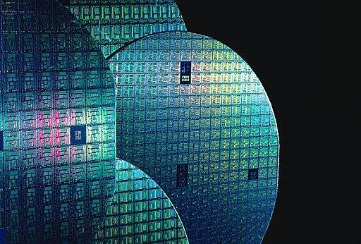
In the realm of electronic and semiconductor components, precise control over material properties is paramount. Tailored conductivity, resistivity, and dielectric properties are meticulously engineered to meet the specific demands of these applications. The ability to fine-tune these properties allows for the creation of components that exhibit optimal performance in various electronic devices.
For instance, in semiconductor manufacturing, the conductivity of materials must be carefully managed to ensure efficient electron flow, while resistivity is crucial for managing heat dissipation and preventing short circuits. Dielectric properties, on the other hand, are essential for insulating layers that prevent electrical crosstalk between adjacent components.
| Property | Importance in Electronics and Semiconductors |
|---|---|
| Conductivity | Ensures efficient electron flow |
| Resistivity | Manages heat dissipation and prevents short circuits |
| Dielectric Properties | Provides insulation and prevents electrical crosstalk |
These tailored properties are not merely theoretical constructs but are integral to the functionality and reliability of modern electronic devices. From microprocessors to integrated circuits, the precision in material engineering translates into enhanced performance and longevity of the final products.
Hard and Decorative Coatings
Building hard and decorative coatings on various surfaces is a critical application of PVD sputtering technology. These coatings are essential for enhancing the durability and aesthetic appeal of wear surfaces, tools, and consumer products.
Applications in Wear Surfaces
In wear surfaces, such as cutting tools and mechanical components, hard coatings are applied to increase resistance to abrasion, corrosion, and wear. These coatings often consist of materials like titanium nitride (TiN), chromium nitride (CrN), and diamond-like carbon (DLC), which provide superior hardness and wear resistance. For instance, TiN coatings are widely used in cutting tools due to their high hardness and low friction properties, significantly extending the tool life and improving machining efficiency.
Decorative Coatings in Consumer Products
On the other hand, decorative coatings are utilized to enhance the visual appeal of consumer products. These coatings can range from metallic finishes to colorful patterns, providing a wide array of aesthetic options. For example, PVD coatings are commonly used in the production of high-end watches, jewelry, and household items. The process allows for the creation of durable, scratch-resistant surfaces that maintain their luster over time, making them ideal for long-lasting consumer goods.
Tools and Industrial Applications
In tools and industrial applications, the combination of hard and decorative coatings can offer dual benefits. Tools such as drills, saws, and dies can be coated with hard materials to improve their performance and lifespan, while decorative coatings can be applied to industrial equipment to enhance their appearance and brand identity. This dual approach ensures that both functionality and aesthetics are optimized, catering to the demands of modern industrial applications.
By leveraging PVD sputtering technology, manufacturers can create tailored coatings that meet specific performance and aesthetic requirements, driving innovation in various industries.
Optical Applications
Optical applications of PVD sputtering technology extend beyond mere transmission and reflection modulation. These applications are pivotal in enhancing the functionality of optical lenses, filters, mirrors, and even architectural or automotive glass. By precisely controlling the deposition of thin films, engineers can tailor the optical properties of these materials to meet specific requirements.
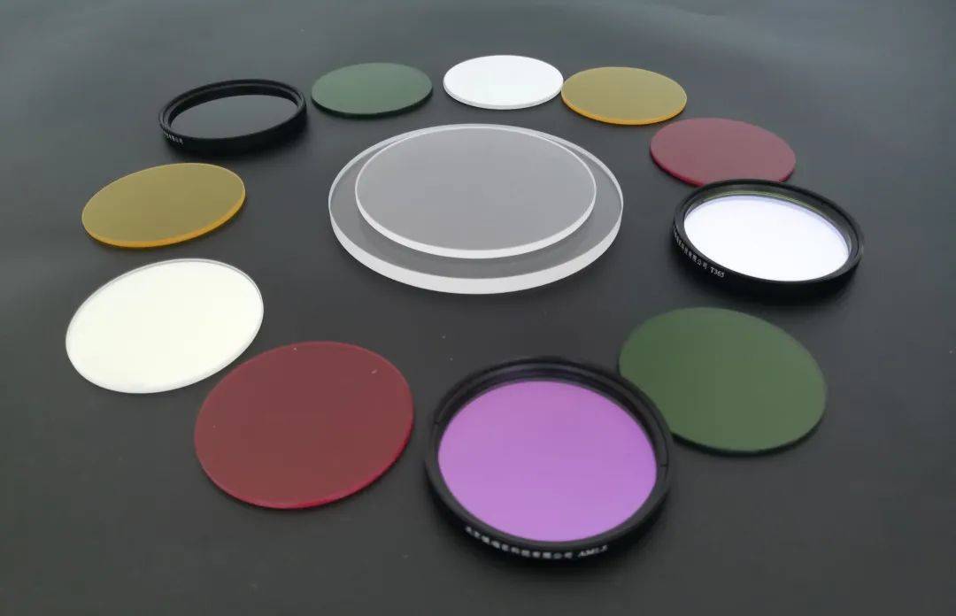
For instance, in optical lenses, the deposition of specific coatings can reduce glare and improve light transmission, enhancing the clarity and efficiency of the lens. Similarly, filters can be designed to block or pass particular wavelengths, making them indispensable in various imaging and spectroscopic applications.
In the realm of architectural glass, PVD sputtering allows for the creation of smart glass that can adjust its transparency based on environmental conditions or user preferences. This technology not only provides aesthetic benefits but also contributes to energy efficiency by reducing the need for artificial lighting and HVAC systems.
Automotive glass benefits from these advancements as well. By modulating the absorption and reflection wavelengths, PVD sputtering can enhance the durability and safety of windshields and side windows. This technology can also be used to create self-cleaning and anti-fog coatings, improving both the driving experience and vehicle maintenance.
In summary, the optical applications of PVD sputtering technology are diverse and impactful, influencing sectors ranging from consumer electronics to automotive and architectural industries.
Energy Harvesting
Energy harvesting, particularly through photovoltaic solar panels and solar towers, represents a cornerstone in the transition towards renewable energy sources. These technologies are pivotal in converting sunlight into usable electrical energy, thereby reducing dependency on fossil fuels and mitigating environmental impacts.
Photovoltaic solar panels operate on the principle of photovoltaic effect, where photons from sunlight are absorbed by semiconductor materials, generating electric current. This method is versatile, applicable in both large-scale power plants and small-scale, decentralized energy solutions. The efficiency of these panels has seen significant improvements over the years, driven by advancements in material science and manufacturing techniques.
Solar towers, on the other hand, utilize concentrated solar power (CSP) technology. They work by focusing sunlight onto a receiver positioned at the top of a tower, which heats a fluid to produce steam. This steam then drives a turbine to generate electricity. This method offers the advantage of energy storage, as the heated fluid can be retained and used to generate power even after sunset or during periods of low sunlight.
Both technologies contribute to a sustainable energy future, offering scalable solutions that can be tailored to meet diverse energy demands. The integration of these harvesting methods with PVD sputtering technology, which enhances the performance of photovoltaic cells, further underscores their significance in modern energy systems.
Components of Thin Film Sputtering Process
Substrate
The substrate plays a pivotal role in the thin film deposition process, serving as the foundational surface to which the thin film functionality is applied. This surface can be made from a variety of materials, including metals, ceramics, and even polymers, each chosen based on the specific requirements of the application. For instance, in the production of electronic and semiconductor components, substrates like silicon wafers are commonly used due to their compatibility with the high-precision demands of these industries.
In the context of hard and decorative coatings, the substrate might be a tool or a consumer product, where the goal is to enhance durability or aesthetic appeal. In optical applications, substrates such as glass or specialized lenses are utilized to modulate light transmission, reflection, or absorption. Each type of substrate brings its own set of challenges and considerations, particularly in terms of surface preparation and adhesion, which are critical to the successful deposition of a uniform and functional thin film.
The choice of substrate is not merely about the material but also about its geometry and surface texture. For example, in energy harvesting through photovoltaic solar panels, the substrate must be able to withstand outdoor conditions while efficiently converting sunlight into electricity. This necessitates a robust material with excellent thermal and environmental stability.
Overall, the substrate is a foundational element in the PVD sputtering process, influencing not only the properties of the final product but also the efficiency and effectiveness of the deposition process itself.
Target
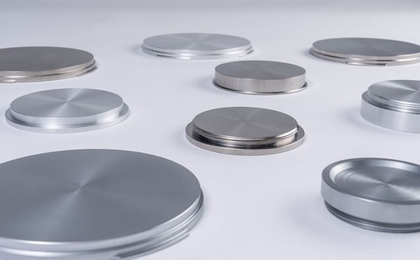
The target in the PVD sputtering process is a critical component that serves as the source of material for the deposition onto the substrate. This material, often in the form of a solid block or disc, is composed of the desired elements or compounds that will form the thin film on the substrate. The target's composition directly influences the properties of the resulting film, making it a key determinant in achieving specific functionalities such as enhanced conductivity, durability, or optical properties.
In the context of electronic and semiconductor applications, the target material must exhibit precise electrical properties, while for hard and decorative coatings, it may need to provide exceptional wear resistance or aesthetic appeal. For optical applications, the target's material properties are tailored to modulate light transmission, reflection, or absorption. In energy harvesting, the target's composition is crucial for optimizing the efficiency of photovoltaic cells.
The selection of the target material is thus a multifaceted decision, balancing the requirements of the application with the capabilities of the sputtering process. The quality and consistency of the target material are paramount, as any impurities or defects can lead to non-uniformities in the deposited film, affecting the overall performance of the final product.
Vacuum Chamber
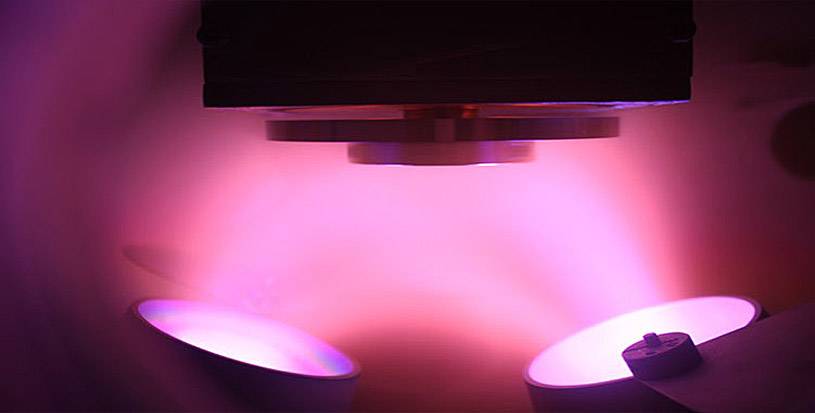
The vacuum chamber is a critical component in the thin film sputtering process, designed to create an environment where precise control over pressure and atmosphere is essential. This enclosed space is engineered to remove air and pressure, allowing for the testing and application of materials under vacuum conditions. The chamber's design is multifaceted, involving careful selection of materials and shapes to ensure it can withstand the drastic changes in pressure inherent to vacuum environments.
Materials and Design
Vacuum chambers are typically constructed from materials like steel alloys and stainless steel, which are chosen for their strength and ability to resist pressure changes. However, the flexibility in material choice is broad; chambers can also be made from glass, plastic, aluminum, brass, high-density ceramics, and acrylic. This diversity in materials is due to the unique requirements of each application, whether it's for educational purposes, industrial testing, or specialized manufacturing processes.
Shapes and Applications
The shape of a vacuum chamber can vary significantly, ranging from the familiar small glass chambers seen in classrooms to larger, more complex designs such as vertical or horizontal cylinders, spheres, and rectangular boxes. Each shape offers distinct advantages depending on the specific needs of the experiment or manufacturing process it supports. For instance, a spherical chamber might provide uniform stress distribution, while a cylindrical one could facilitate easier access and maintenance.
In industrial applications, vacuum chambers are indispensable for high-altitude testing, drying, and offgassing, ensuring the quality and durability of products. In the aerospace industry, they are crucial for simulating the conditions of space, testing components' ability to withstand the vacuum and pressure of orbit. Additionally, vacuum chambers are used across various industries to determine the stability of packaging that may be subjected to air travel, ensuring products remain intact during transit.
The vacuum chamber, with its sophisticated hardware and software, plays a pivotal role in maintaining and controlling the delicate balance required for successful thin film sputtering processes. Its ability to create and sustain a controlled vacuum environment is what enables the precise application of thin films onto substrates, making it an essential tool in modern manufacturing and research.
Hot Isostatic Pressing (HIP) in Target Production
Powdered Metals, Ceramics, and Compounds
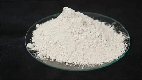
In the production of sputtering targets, materials such as powdered metals, ceramics, intermetallics, and compounds play a pivotal role. These materials are processed into targets through a variety of methods, each tailored to enhance specific properties required for different applications.
Types of Powdered Materials
- Powdered Metals: These are typically used for their excellent electrical and thermal conductivity, making them ideal for applications in electronic and semiconductor components.
- Ceramics: Known for their high hardness and wear resistance, ceramics are often employed in hard coatings and optical applications.
- Intermetallics: These compounds offer a unique combination of properties, such as high strength and thermal stability, which are crucial for aerospace and energy harvesting technologies.
- Compounds: A broad category that includes a variety of materials, each with specific properties that can be modulated for different applications, from decorative coatings to energy-efficient glass.
Processing Techniques
The transformation of these powdered materials into sputtering targets involves several advanced techniques, each designed to optimize the target's performance:
- Hot Isostatic Pressing (HIP): This method compresses the powdered material under high pressure and temperature, resulting in a dense, homogeneous target with minimal porosity.
- Sintering: A process that heats the powdered material to just below its melting point, causing the particles to bond without fully melting, producing a strong, yet porous target.
- Spray Forming: Involves spraying molten material onto a substrate, rapidly solidifying it into a target with fine microstructure and high density.
Each of these techniques contributes to the creation of targets that are optimized for specific applications within the PVD sputtering process, ensuring high performance and reliability.
Improved Cast, Sintered, or Sprayed Targets
The production of sputtering targets can be significantly enhanced through various manufacturing techniques such as casting, sintering, and thermal spraying. Each method offers unique advantages and challenges, tailored to specific materials and applications.
Cast Targets: These targets benefit from high compositional and microstructural consistency, ensuring purity control, which translates to high process yield and extended target life. Commonly used materials include InSn, Sn alloys, ZnAl, and ZnSn. Despite these advantages, casting is limited to well-behaved metals and stable alloys that can withstand successive thermo-mechanical processing without degrading.
Sintered Targets: Hot Isostatic Pressing (HIP) is a key technique in producing sintered targets, offering superior grain structure. However, this method is not without risks; oxygen contamination (particularly in metal mode), anomalous erosion, and particle formation must be closely monitored. HIP products include Cr, Mo, ITO, AZO, and ZnO sputtering targets, each requiring precise handling to mitigate these risks.
Sprayed Targets: Thermal spraying, provided by companies like KINTEK, offers a versatile solution for producing rotary targets. This method ensures optimal process stability and performance through techniques such as plasma, arc, and cold spray. The primary materials include AZO, ITO, Mo, Si, TiOx, ZnO, and ZTO. Despite the advantages, the intense bombardment and reactive nature of the process can lead to common failures such as cracking in fragile metals like Silicon and Germanium, deformation in hard metals like Niobium and Zirconium, and compositional changes in complex alloys.
Extruded Targets: KINTEK also supplies high-purity extruded targets made from materials such as Al, Cu, Mo, Nb, Ta, Ti, Zr, and V. These targets maintain good purity and grain size, making them suitable for a variety of applications.
To address these challenges, Materion employs a comprehensive range of powder and plate manufacturing technologies, coupled with years of expertise in handling thin film deposition materials. This holistic approach ensures that even the most challenging applications can be effectively addressed, enhancing the overall performance and reliability of sputtering targets.
Diffusion Bonding
Diffusion bonding has long been employed to join high-strength and refractory metals, which are often challenging or impossible to weld using conventional methods. This process involves applying both high temperature and pressure to similar or dissimilar metals that are mated together in a hot press. Under these conditions, the atoms on the solid metallic surfaces intersperse and bond, creating a strong and temperature-resistant joint. This method stands out from traditional brazing techniques as it does not require filler materials, thereby preserving the original weight and dimensions of the mated metals.
The strength and temperature resistance of the resulting bond are intrinsic to the base metals themselves, making diffusion bonding particularly advantageous for applications involving refractory and high-strength alloyed materials. Whether used to bond layers or simply to join two parts, this technique offers a robust solution for creating durable and efficient metal assemblies.
In recent years, advancements in the precision control of temperature and the uniformity of pressure across large parts have further expanded the potential applications of diffusion bonding. This has opened up new possibilities for the production of next-generation products, particularly in industries where high-performance materials are critical.
Understanding PVD and Sputtering Technology
Historical Context
The evolution of PVD (Physical Vapor Deposition) and sputtering technology is deeply rooted in the pioneering work of several key figures in the 19th and 20th centuries. One of the earliest significant contributions was made by Sir William Robert Grove, a British scientist who, in the mid-19th century, conducted experiments with electrical discharges in rarefied gases, laying the groundwork for what would later become sputtering technology. Grove's work was foundational in understanding the behavior of particles in low-pressure environments, which is critical for the sputtering process.
Following Grove, Michael Faraday, another British physicist, made substantial advancements in the field. Faraday's studies on the deposition of metals in vacuum environments provided insights into the mechanisms of film formation, which are essential for the development of PVD techniques. His experiments with cathode rays and the discovery of the Faraday dark space further elucidated the principles underlying sputtering.
In the early 20th century, the American physicist Irving Langmuir made significant contributions to the field, particularly with his work on the behavior of electrons in gases. Langmuir's research helped to refine the understanding of plasma physics, which is crucial for the operation of sputtering systems.
The modern era of sputtering technology began with the work of William Wright, who, in 1967, developed the first practical magnetron sputtering system. Wright's innovation allowed for more efficient and controllable deposition of thin films, significantly advancing the application of sputtering in various industries. His work marked a pivotal moment in the transition from laboratory curiosities to industrial processes.
These historical developments collectively set the stage for the sophisticated PVD and sputtering technologies we rely on today, enabling the production of high-quality thin films for a wide array of applications, from electronics to optics and beyond.
Types of Sputtering Techniques
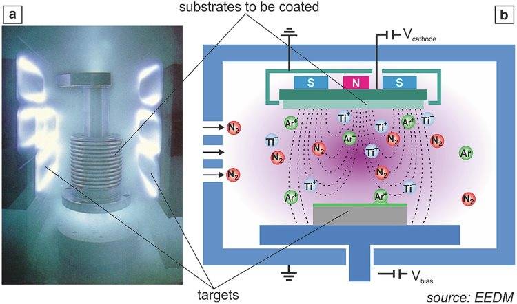
Sputtering techniques are integral to Physical Vapor Deposition (PVD) processes, offering a versatile range of methods to deposit thin films onto various substrates. The primary techniques include Direct Current (DC) magnetron sputtering, Radio Frequency (RF) sputtering, and ion beam sputtering, each tailored to specific applications and material types.
Direct Current (DC) Magnetron Sputtering is widely used for depositing metals and some ceramics. In this method, a direct current power supply generates a plasma in a low-pressure gas environment. The plasma, created near the target material, causes gas ions to collide with the target, dislodging atoms that are then ejected into the gas phase. The magnetic field produced by the magnet assembly enhances the sputtering rate and ensures a more uniform deposition onto the substrate. The sputtering rate can be calculated using a specific formula, which factors in parameters like ion flux density, target material properties, and distance between the target and substrate.
Radio Frequency (RF) Sputtering extends the applicability of sputtering to non-conductive materials. Unlike DC sputtering, RF sputtering uses an alternating current, enabling the deposition of insulating materials. This technique is particularly useful for materials that cannot be sputtered using DC methods, broadening the scope of PVD applications.
Ion Beam Sputtering involves the use of a focused ion beam to bombard the target material, causing atoms to be ejected and deposited onto the substrate. This method offers high precision and control, making it suitable for applications requiring intricate patterns or high-quality coatings.
Each of these techniques has unique advantages and is selected based on the specific requirements of the application, whether it be for electronic components, optical coatings, or energy harvesting devices. Understanding these techniques is crucial for optimizing the PVD process and achieving the desired film properties.
Reactive Sputtering
Reactive sputtering is a sophisticated technique employed in Physical Vapor Deposition (PVD) to create thin film coatings with precisely controlled stoichiometry and structure. This method involves the introduction of reactive gases into the sputtering chamber, such as oxygen or nitrogen, which react with the sputtered particles from a target material to form oxide or nitride films, respectively. The addition of these reactive gases significantly alters the deposition process, making it more complex and requiring careful control of parameters like the partial pressures of both the inert and reactive gases to achieve the desired film composition and properties.
The complexity arises from the hysteresis-like behavior observed in many reactive sputtering processes, necessitating precise control over variables such as gas flow rates and relative pressures. For instance, the Berg Model, proposed by Berg et al., provides a framework for estimating the impact of reactive gas addition on target erosion and film deposition rates. This model helps in understanding how changes in the relative pressures of inert and reactive gases can influence film stoichiometry, which is crucial for optimizing functional properties like stress in silicon nitride (SiNx) films and the refractive index of silicon oxide (SiOx) films.
In practice, reactive sputtering allows for the production of thin films with tailored chemical compositions, enhancing their performance in various applications. For example, in the semiconductor industry, these films can be customized to achieve specific conductivity, resistivity, and dielectric properties, while in optical applications, they can modulate transmission, reflection, and absorption wavelengths. This versatility makes reactive sputtering an indispensable tool in modern PVD technology, enabling the creation of advanced materials with unique properties for a wide range of industries.
Target Geometries and Their Advantages
Planar Targets
Planar targets are widely used in various applications due to their simplicity and effectiveness in material transfer processes. These targets are particularly advantageous in scenarios where the focus is on prototyping or elemental experimentation, especially when the requirement for material is modest. The straightforward geometry of planar targets allows for easy integration into existing sputtering systems, making them a popular choice for initial trials and small-scale production runs.
Advantages of Planar Targets
- Simplicity: The flat, uncomplicated design of planar targets simplifies both the manufacturing process and the integration into sputtering systems. This ease of use is particularly beneficial for researchers and engineers who are testing new materials or processes.
- Cost-Effective: Due to their simple geometry, planar targets can be produced at a lower cost compared to more complex target designs. This makes them an attractive option for projects with limited budgets.
- Versatility: Planar targets can be made from a variety of materials, including metals, ceramics, and compounds, allowing for a wide range of experimental setups and applications.
Disadvantages of Planar Targets
- Material Utilization: One of the primary drawbacks of planar targets is their relatively low material utilization efficiency. The flat surface can lead to uneven wear patterns, resulting in material wastage and the need for frequent replacements.
- Scale Limitations: Planar targets are less suitable for large-scale production due to their limited material transfer capabilities. Their design does not efficiently handle the continuous and high-volume demands typically associated with industrial applications.
- Wear Patterns: The uniform wear across the planar surface can lead to premature degradation, necessitating more frequent maintenance and replacement cycles. This can be a significant disadvantage in high-throughput environments.
In summary, while planar targets offer simplicity and cost-effectiveness, they are best suited for small-scale applications and initial experimentation. Their limitations in material utilization and scalability make them less ideal for large-scale industrial production.
Rotating Targets
The development of rotating targets has significantly enhanced the efficiency and effectiveness of sputtering processes, particularly in large-scale manufacturing applications such as architectural glass and flat panel displays. Unlike traditional planar targets, rotating targets are designed to maximize material utilization and operational longevity.
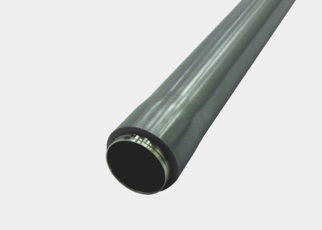
One of the primary advantages of rotating targets is their superior material capacity. These targets typically hold more material, allowing for extended production runs without the need for frequent replacements. This translates to reduced system downtime and increased throughput of coating equipment. For instance, a rotating target can sustain a production run that is several times longer than that of a planar target, thereby enhancing overall productivity.
Moreover, rotating targets facilitate the use of higher power densities during the sputtering process. The continuous rotation of the target ensures that heat buildup is evenly distributed across its surface, mitigating local overheating and extending the target's lifespan. This even distribution of heat also allows for faster deposition rates, as the target can withstand higher energy inputs without compromising its structural integrity. Consequently, the use of rotating targets not only improves the efficiency of the sputtering process but also enhances the quality of the deposited films.
In reactive sputtering, where the target material reacts with a reactive gas to form a desired thin film, rotating targets offer additional benefits. The uniform heat distribution and higher power densities enable more controlled and consistent reactions, leading to superior film properties such as better adhesion, lower porosity, and improved mechanical strength. This makes rotating targets an indispensable tool in industries that require high-precision coatings with exacting standards.
Overall, the adoption of rotating targets in sputtering technology represents a significant advancement, offering tangible benefits in terms of material utilization, process efficiency, and product quality.
Related Products
- Warm Isostatic Press WIP Workstation 300Mpa for High Pressure Applications
- Warm Isostatic Press for Solid State Battery Research
- Electric Split Lab Cold Isostatic Press CIP Machine for Cold Isostatic Pressing
- Manual Cold Isostatic Pressing Machine CIP Pellet Press
- Cold Isostatic Pressing Machine CIP for Small Workpiece Production 400Mpa
Related Articles
- Beyond the Spec Sheet: Mastering the Thermal Dynamics of Warm Isostatic Pressing
- Comprehensive Overview of Warm Isostatic Press and Its Applications
- How to Achieve Uniform Pressure with Warm Isostatic Press
- Warm Isostatic Pressing An Overview of the Process and Equipment
- Key Factors to Consider When Using Warm Isostatic Press
