Introduction to Magnetron Sputtering
Overview of Magnetron Sputtering
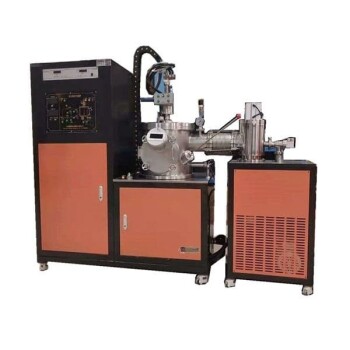
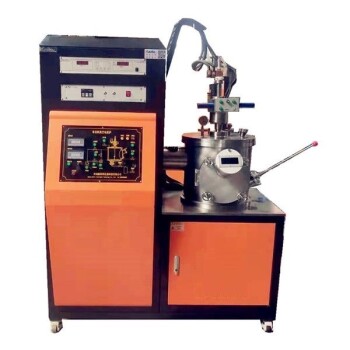
Magnetron sputtering is a sophisticated thin film preparation technique that involves the ejection of atoms or molecules from a target material in a vacuum environment. These ejected particles are then deposited onto a substrate, forming a thin film. The process can be broadly classified into three main types based on the frequency of the power supply used: DC sputtering, mid-frequency (MF) sputtering, and radio frequency (RF) sputtering.
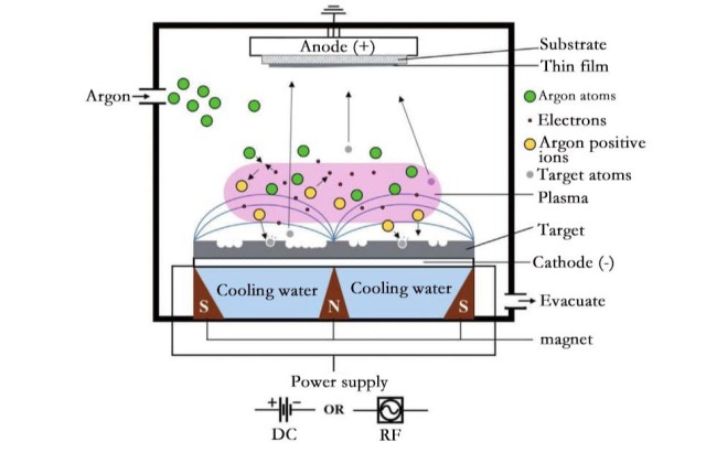
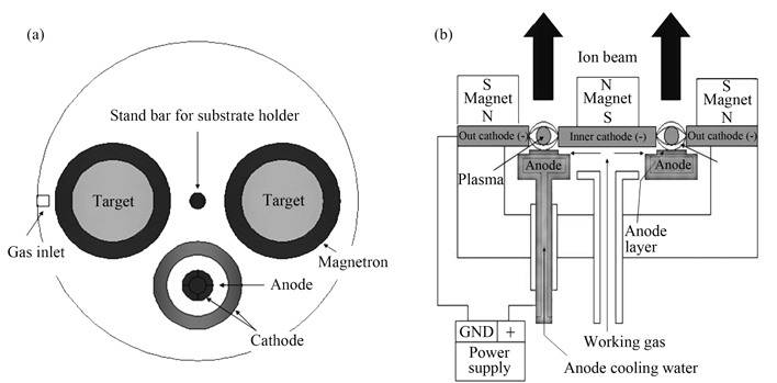
The fundamental concept behind magnetron sputtering is relatively straightforward, yet the underlying mechanisms are quite complex. One of the key distinguishing features of magnetron sputtering, compared to basic diode or DC sputtering systems, is the introduction of a strong magnetic field near the target area. This magnetic field plays a crucial role in the process by causing electrons to spiral along magnetic flux lines, thereby confining the plasma to a region very close to the target. This confinement prevents the plasma from damaging the thin film being formed on the substrate.
In a typical magnetron sputtering setup, a chamber is first evacuated to a high vacuum to minimize background gas and potential contaminants. Subsequently, a sputtering gas, which forms the plasma, is introduced into the chamber, and the pressure is regulated to the milliTorr range. The plasma, generated by the interaction of the sputtering gas with the target material, results in the erosion of the target's surface by high-energy ions. These liberated atoms then travel through the vacuum and deposit onto the substrate, forming the desired thin film.
The addition of a magnetic field in magnetron sputtering not only enhances the efficiency of the process but also allows for more controlled and uniform film deposition. This makes magnetron sputtering a preferred method for applications requiring high-quality, uniform, and dense thin films.
Types of Sputtering Techniques
DC Sputtering
DC sputtering is a foundational technique within the realm of thin-film Physical Vapor Deposition (PVD) coating processes. It operates by employing a Direct Current (DC) power supply to ionize the target material, thereby generating a plasma on its surface. This plasma is crucial as it facilitates the acceleration of ions, which subsequently bombard the target material. This energetic bombardment results in the release of atoms or molecules from the target, which then condense onto a nearby substrate to form a thin film.
One of the standout features of DC sputtering is its simplicity and cost-effectiveness, making it an ideal choice for basic film preparations and applications where precise deposition rate control is not paramount. This technique is widely utilized across various industries, including the semiconductor sector for microchip circuitry, and in decorative applications such as gold coatings on jewelry and watches. Additionally, DC sputtering finds utility in creating non-reflective coatings on glass and optical components, as well as in the production of metalized packaging plastics.
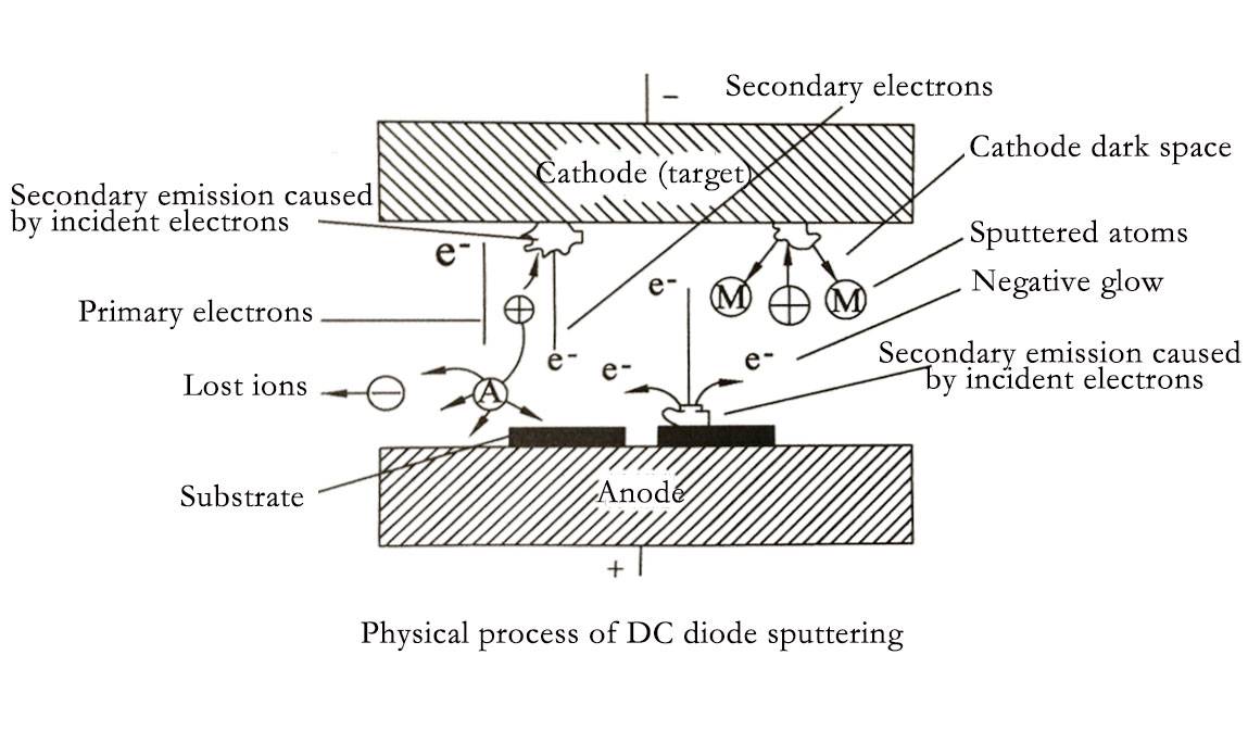
The process of DC sputtering begins with the application of a voltage to a metal target in a low-pressure gas environment, typically argon. The gas ions, upon collision with the target, eject microscopic particles of the target material, which are then deposited onto the substrate. This method ensures a straightforward and economical approach to metal deposition, particularly for coating electrically conductive target materials.
In summary, DC sputtering stands out as a versatile and accessible method for thin-film deposition, offering a balanced mix of simplicity, cost-effectiveness, and broad applicability across diverse industries.
Mid-Frequency Sputtering
Mid-frequency sputtering leverages a power supply operating at frequencies typically between 50 kHz and 5 MHz to generate a stable plasma environment. This frequency range is strategically chosen because it allows for a balance between ion and electron dynamics, ensuring that ions can still follow the alternating field while electrons contribute to the plasma density. The result is a plasma with higher ion bombardment energy compared to DC sputtering, which translates to a more controlled and uniform deposition rate.
In mid-frequency sputtering, the alternating field accelerates both ions and electrons, but due to the ions' smaller charge-to-mass ratio, they begin to lag at frequencies above approximately 50 kHz. This lag is beneficial as it enhances the ion bombardment on the target, leading to a more efficient release of atoms or molecules. The electrons, on the other hand, oscillate within the plasma, increasing the collision frequency with argon atoms and thereby boosting the plasma rate. This increased plasma rate allows for lower operating pressures, typically in the range of 10^-1 to 10^-2 Pa, while maintaining a high sputtering rate.
The lower pressure environment in mid-frequency sputtering facilitates the formation of thin films with distinct microstructures that are not achievable at higher pressures. This method is particularly advantageous for preparing high-quality films with properties such as high deposition rates, excellent uniformity, and minimal internal stress. These characteristics make mid-frequency sputtering ideal for applications in optical films, magnetic films, and transparent conductive films, where precision and uniformity are paramount.
| Parameter | Mid-Frequency Sputtering |
|---|---|
| Power Supply Frequency | 50 kHz - 5 MHz |
| Ion Bombardment Energy | Higher compared to DC sputtering |
| Deposition Rate | More stable and uniform |
| Operating Pressure | 10^-1 to 10^-2 Pa |
| Applications | Optical films, magnetic films, transparent conductive films |
Radio Frequency Sputtering
Radio Frequency Sputtering (RF Sputtering) is a sophisticated technique that employs a radio frequency power supply, typically operating at 13.56 MHz, to create a stable plasma environment. This method is particularly advantageous for the deposition of insulating materials, which are inherently non-conductive. The process involves alternating the electrical potential at radio frequencies, which effectively "cleans" the target material's surface by preventing charge build-up. During the positive cycle, electrons are attracted to the target, giving it a negative bias, while during the negative cycle, ion bombardment continues unabated.
This technique ensures that the target material remains free from charge accumulation, which is crucial for maintaining the uniformity and density of the deposited films. The use of RF Sputtering is highly beneficial in environments where insulating materials need to be coated without compromising the quality of the film. The ability to control the plasma and the ion bombardment energy precisely results in films that are not only uniform but also exceptionally dense, making RF Sputtering ideal for applications requiring high-quality and high-uniformity films.
RF Sputtering has been utilized since the 1960s, with early applications including the deposition of SiO₂ films on silicon substrates by the BM Company in the United States. The historical and technological advancements in this field underscore its reliability and effectiveness in producing high-performance films, such as metal films, alloy films, piezoelectric films, ferroelectric films, and high-temperature superconducting films.
Applications and Characteristics of Different Sputtering Methods
DC Sputtering Applications
DC Sputtering is a versatile technique that excels in creating thin films with specific properties tailored for various industrial applications. These films often exhibit either amorphous or microcrystalline crystal structures, which contribute to their unique mechanical and chemical characteristics.
One of the standout features of DC Sputtering films is their high internal stress. This property makes them particularly suitable for wear-resistant coatings, where durability and resistance to mechanical abrasion are paramount. For instance, in the semiconductor industry, DC Sputtering is used to create microchip circuitry on the molecular level, ensuring that the films can withstand the rigors of production and operation.

In addition to wear resistance, DC Sputtering is also adept at producing antioxidant films. These films are crucial in environments where materials are exposed to oxidative conditions, such as in certain chemical processing or high-temperature applications. The ability to create surface films with specific microstructures further enhances their utility, making them ideal for a range of surface engineering applications.
DC Sputtering is not limited to industrial uses; it also finds applications in consumer goods. For example, it is used for gold sputter coatings on jewelry, watches, and other decorative items, providing a lustrous finish that is both durable and aesthetically pleasing. Similarly, non-reflective coatings on glass and optical components are another area where DC Sputtering shines, enhancing the functionality and performance of these products.
Moreover, DC Sputtering is employed in the creation of metalized packaging plastics, which are essential for food packaging and other applications requiring a barrier against moisture and gases. The ability to control and optimize the deposition process with DC power makes it a cost-effective and reliable choice for these applications.
In summary, DC Sputtering's ability to produce films with controlled internal stress, tailored microstructures, and specific mechanical properties makes it a valuable tool across multiple industries, from semiconductors to consumer goods.
Mid-Frequency Sputtering Applications
Mid-frequency sputtering stands out for its ability to produce high-quality films with a high deposition rate, exceptional uniformity, and minimal internal stress. This technique is particularly well-suited for a variety of advanced film applications, including optical films, magnetic films, and transparent conductive films.
One of the key advantages of mid-frequency sputtering is its ability to handle materials that require precise control over the deposition process. For instance, optical films demand a high degree of uniformity and low internal stress to ensure optimal performance in devices such as lenses and mirrors. Magnetic films, used in data storage and magnetic sensors, benefit from the high deposition rate and low stress, which contribute to their durability and performance. Similarly, transparent conductive films, essential in touchscreens and solar cells, require both high transparency and conductivity, which mid-frequency sputtering can deliver effectively.

The use of mid-frequency power in sputtering allows for a stable plasma environment, enhancing the ion bombardment energy and leading to more controlled and uniform film deposition. This stability is crucial for the preparation of films that must meet stringent performance criteria, making mid-frequency sputtering an indispensable tool in the production of advanced thin films.
RF Sputtering Applications
RF sputtering has emerged as a versatile and indispensable technique in various high-tech industries, owing to its ability to produce high-density, high-uniformity films. This method is particularly favored for creating high-quality and high-performance films such as metal films, alloy films, piezoelectric films, ferroelectric films, and high-temperature superconducting films. The unique advantages of RF sputtering, such as lower chamber pressure and the use of radio frequency power supply, make it ideal for handling target materials with insulating qualities, which are often challenging for alternative methods like DC sputtering.
One of the most significant advancements in RF sputtering is its application in the deposition of highly insulating oxides. These oxides, including aluminium oxide, tantalum oxide, and silicon oxide, are crucial for enhancing the performance of microchip circuitry in the computer and semiconductor industries. By carefully controlling the deposition process, RF sputtering ensures that these insulating layers are uniformly applied between metallic target surfaces, thereby improving the overall efficiency and reliability of the devices.
The demand for RF sputtered films is expected to surge in the coming years, driven by the increasing need for miniaturization in thin-film devices and the advancements in nano-technological applications. This growth is not limited to the semiconductor sector but extends to diverse fields such as energy, optoelectronics, life sciences, mechanics, and the chemical industry. The adaptability and precision of RF sputtering make it a go-to technique for a wide array of applications, solidifying its position as a cornerstone technology in modern manufacturing processes.
Related Products
- RF PECVD System Radio Frequency Plasma-Enhanced Chemical Vapor Deposition RF PECVD
- Inclined Rotary Plasma Enhanced Chemical Vapor Deposition PECVD Equipment Tube Furnace Machine
- Inclined Rotary Plasma Enhanced Chemical Vapor Deposition PECVD Equipment Tube Furnace Machine
- Microwave Plasma Chemical Vapor Deposition MPCVD Machine System Reactor for Lab and Diamond Growth
- Chemical Vapor Deposition CVD Equipment System Chamber Slide PECVD Tube Furnace with Liquid Gasifier PECVD Machine
Related Articles
- An Introduction to Chemical Vapor Deposition (CVD)
- Comparing the Performance of PECVD and HPCVD in Coating Applications
- Plasma Enhanced Chemical Vapor Deposition (PECVD): A Comprehensive Guide
- Understanding PECVD: A Guide to Plasma-Enhanced Chemical Vapor Deposition
- The Role of Plasma in PECVD Coatings
